Wednesday, March 4th, 2009
Electron beam direct write (EBDW) lithography is well-developed and has better potential resolution than any other method, but writing speeds did not keep up with Moore’s law after about 1980, leading to abysmal throughput (measured in hours per wafer). Now, the e-Beam Initiative focusing on design for e-beam manufacturing (DFEB) and multibeam writing using MEMS technology promise to make it practical, at least for prototyping and short production runs.
A group of 20 leading companies announced the launch of the eBeam Initiative, a forum dedicated to explaining and promoting design for e-beam (DFEB) on February 24. D2S serves as the managing sponsor of Initiative. The formal steering group for the eBeam Initiative consists of Advantest, CEA/Leti, D2S, e-Shuttle, Fujitsu Microelectronics, and Vistec. Practical e-beam manufacturing would also reduce the need for round-A fabless companies to invest in mask sets. One goal of the eBeam initiative would be to establish e-Beam foundries serving those markets. At present, there are very few.
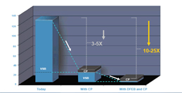
 The enabling technology for the eBeam initiative is character projection (CP), where the electron beam is shaped by a stencil near the source and then demagnified, forming an image on the wafer (Ref: BetaBlog 090126). Using CP instead of a variable-shaped beam (VSB) improves writing time by 3-5X. If the designs are optimized for character projection, the throughput improvement becomes 10-25X (see figure), and such designs could print at 1 wph, according to Fujimura.
The throughput problem in EBDW results directly from Coulomb’s law: put enough electrons into a high resolution “pencil” beam to expose resist quickly and their electric fields will push them apart, ruining everything. Of the solutions that use a great many low current beams in parallel, Mapper Lithography from Holland is, perhaps, the furthest along. The 50kV PML2 system from IMS Nanofabrication AG of Austria has 43,000 beams working in an alpha-tool. With DARPA support, KLA-Tencor has entered its Reflective e-beam lithography (REBL) Nanowriter in the world-wide competition. Details about these technologies, and additional perspectives regarding the eBeam Initiative will be in the next issue of the BetaSights Newsletter. –M.D.L.
