Monday, March 2nd, 2009
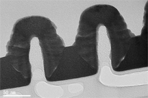
Partners SII NanoTechnology and Carl Zeiss NTS have joined with ASML R&D and Toshiba’s process and manufacturing engineering groups to show a new way to create accurate cross-sections of soft photoresist and low-k dielectric lines in dense circuit patterns. First shown in a poster paper at SPIE last week was the ability to generate accurate 2D profiles for <45nm resist lines, using argon-beam induced deposition (ArBID) of a thin tungsten (W) coating (see figure).
Physical cross-sections of structures are required to calibrate other metrology tools (whether CD-SEM or scatterometry), and it is inherently challening to cut a soft material without smearing the edges. Even at the nanoscale where the cut is done with a focused ion beam (FIB) inside of a scanning electron microscope (SEM) chamber, when every nm counts it is difficult to not distort shapes. A thin coating of metal over the surface has traditionally been used to preserve soft strucutres, and until the 45nm node the process of record was platinum (Pt) deposited in the e-beam column of the SEM. However, 15-20% shrinkage in 45nm node resist line heights has been seen due to the e-beam coating, so a more gentle metal deposition was needed.
A TripleBeam metrology system consists of SEM, FIB, and Argon columns. The SEM column is mainly used for imaging, the FIB column is used for material removal, deposition, and imaging (e.g. grain boundaries in metals), while the Ar column cleans and does small amounts of removal and deposition. The Argon column has a relatively large spot size compared to a FIB, and so the local species flux is relatively small. Using a static Ar beam at 600V and 2.5 nA to minimize the local dose rate for tungsten (W) deposition, scanning transmission electron microscope (STEM) images of 45 nm dense lines (photoresist on BARC) have been made.
Using the FIB in the triple beam system, Toshiba was able to generate TEM images of 55nm dense contact holes. The measured resist height with STEM and scatterometry matches within 3% using ArBID, and can be applied for the calibration of scatterometry models used to control CD after litho and before etch in the fab. 3D metrology using STEM is feasible with good total measurement uncertainty (TMU) after averaging together the data from 50 profiles. Further research is needed to find out if ArBID can be applied for the 32nm node. –E.K.
Tags: 32nm, 45nm, APC, Ar, calibration, FIB, linewidth, metrology, SEM, TEM

