Wednesday, March 11th, 2009
Nanometrics today announced the release of Version 2.0 of its NanoCD Suite of solutions for optical critical dimension (OCD) metrology, just one year after V1 was released. OCD (a.k.a., “scatterometry”) has been used to successfully control fab processes for many years. The major known limitation of the technique is model building from reference metrology data, so Nanometrics has upgraded the software development tools to accelerate model building.

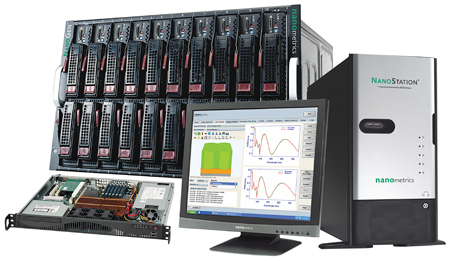
NanoCD Suite (NanoGen, NanoMatch, NanoStation and NanoDiffract) for OCD metrology (source: Nanometrics)
The new OCD suite is made up of components which allow for scalable fab-wide metrology solutions: NanoDiffract, NanoGen, NanoMatch, and NanoStation (see figure). The NanoDiffract is the software that runs in various hardware boxes. NanoGen is an offline server-based library generation system that can support numerous users and systems, while NanoStation is an offline desktop system used for recipe and library generation. NanoMatch is a computer providing real-time analysis that runs within another metrology system: standalone Atlas XP and Atlas-M for wafers and reticles, and the IMPULSE/9010 integrated metrology family.
“Many customers are applying our NanoCD technology for measurements in every sector of the fab, including thin film, CMP, advanced lithography and etch applications on complex 32nm and 22nm node test structures,” commented Nagesh Avadhany, vice president of Applications at Nanometrics. As was reported from SPIE 2008 by this editor, OCD measurement precision of <1% has also been shown for finFET gate stack characterization; measuring in the fin area seems to provide sufficient resolution for process control for both the high-k and metal-gate depositions.
Enhancements in NanoDiffract allow users to control their process based on measurements of key parameters directly on DRAM, Flash, and SRAM cells. This measurement capability allows process engineers to optimize their metrology recipe and determine sensitivity even before initial wafers are processed. This highly optimized workflow for OCD applications development results in much faster time to results leading to claims of rapid production deployment, higher productivity, and lower cost of ownership. –E.K.
Tags: 22nm, 32nm, CD, CMP, etch, fab, finFET, high-k, HK, IC, metal-gate, metrology, MG, OCD
