Thursday, April 23rd, 2009
Silicon Valley has certainly not been immune to the current economic conditions, with many companies announcing multiple rounds of layoffs and moving operations overseas. Yet for many it is still considered “the heart” of the high-tech industry. At today’s well-attended Silicon Valley Lunch Forum, organized by the Sales and Marketing Council of SEMI, three speakers addressed the question of the future of Silicon Valley. Traditional silicon IC design and pilot production work, innovative printed ICs, and photovoltaics fabs are all part of the future.
“It is not the product, or the pricing or the support that has been key to the development of the Valley, but the networking opportunities,” declared Art Zafiropoulo, chairman and CEO of lithography tool maker Ultratech Stepper. In his view, the key challenge to the continued success of Silicon Valley is relatively high tax rates and cumbersome tax regulations. As a result, Zafiropoulo sees a future for Silicon Valley that will still be a high tech center in the areas of design, software and management but will no longer be a center of manufacturing. In fact, “the equipment industry will literally disappear in Silicon Valley and eventually in the United States,” Zafiropoulo predicted.
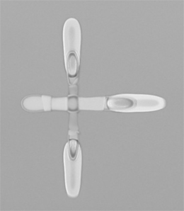
But the other two speakers see a slightly different scenario. Richard Young, vice president of operations for Kovio, a developer of printed silicon electronics, talked about his own company’s commitment to Silicon Valley. With a 22k square foot clean room in Milpitas, “Kovio has every intention of keeping manufacturing here in the valley and will be ramping production this year,” reported Young. While about 90% of all printed semiconductors are based on organic chemistries, Kovio has developed a 100% inorganic silicon printed transistor and was the first company to demonstrate an all-printed transistor as well as the world’s first silicon ink (see figure). According to Young, the printed silicon industry has the potential to one day be as big as the silicon industry is today.
Printed silicon electronics would fall under the category of “non-Moore’s Law products” as outlined by the final speaker, Dave Bergeron, chief technology officer of SVTC, speaking on emerging technologies in a changing market. Working with 200mm diameter wafers, SVTC has three manufacturing facilities, of which two are located in San Jose in the heart of Silicon Valley, a semiconductor fab and a solar fab that will be commission later this year. All facilities have a Class 10 Cleanroom. Most current SVTC customers are not trying to push Moore’s Law. Bergeron says their “sweet spot” is between 90 and 350nm structures. In Bergeron’s view, despite the current economic reality, “innovation will continue and especially in Silicon Valley.” He further explained, “there are a lot of people here in the valley with the background and knowledge to do this, and frankly it can’t get done anywhere else.” –E.S.

