Monday, August 17th, 2009
Luminescent Technologies, Inc., a computational lithography company, has broadened its reach by announcing the industry’s first offline computational photomask inspection product (unofficially named LAIPH for Luminescent Automated Image Processing Hub). A “premier company in Asia” is the first customer to qualify the new computational defect review product in volume production. According to a Luminescent representative, revenue has changed hands, successfully ending the beta-test process.
During ordinary photomask inspection, operators manually sort through and evaluate defect images obtained using optical inspection and defect review tools to determine if anomalies on a photomask will affect wafer yield. This is time consuming, and subject to operator variability. Photomask customers have demanded that all identified defects be repaired, whether or not the inspector deems them printable or not. Luminescent’s computational solution provides automated mask defect review and dispositioning based on aerial images of the photomask. The product accepts images from commonly used mask defect inspection and review tools, enhances the images, and quickly and accurately determines if the defects are critical or not. Operator errors are eliminated and defect review cycle time is significantly reduced, in some instances by greater than 75 percent, according to Luminescent.
Computational defect review of this sort opens a broader field which Luminescent calls “computational lithography and inspection (CLI)”. Computational lithography uses mathematical models to improve the resolution and process window of photolithography imaging without changing the exposure wavelength by adding structures on the mask or altering exposure illumination. Computational Lithography has become the most viable and economical approach for extending optical lithography for several generations, according to Dr. Morris Kori, CEO of Luminescent. Computational inspection integrates with computational lithography by using similar mathematical approaches to filter for photomask defects by simulating pattern errors on final silicon.
In a paper at last April’s Photomask Japan in Yokohama, C. Y. Chen of TSMC E-Beam Operations Division and a team from TSMC and Luminescent described the use of computational inspection methods to analyze the images produced by Zeiss AIMS defect review tools at TSMC’s maskmaking facilities. The AIMS tool finds defect locations flagged by a KLA-Tencor mask inspection system and determines the image that would be projected onto the wafer by that defect using optics and illumination that mimic those of the production stepper.
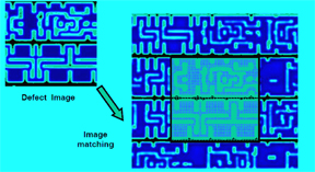
The Luminescent Automated Image Processor Hub (LAIPH, pronounced “life”), then compared the AIMS defect image to a reference image (see figure), accounting for potential tilts and misalignments and determined whether that mask site passed or failed specifications. Both contact and line/space patterns were reviewed automatically and the results correlated with manual measurement of indicated wafer CD error. The Luminescent system correlated essentially perfectly with the operator results, with the discrepancies mainly due to the operator’s inability to identify contact position shift. Throughput improvement using the automatic measurements was significant. An operator took 40 minutes to perform the X/Y measurements on 17 blind or mis-sized contact defects, while it only took LAIPH only 1 minute.
The authors noted that the TSMC EBO processes more than 167 masks per day. On average, there are tens to hundreds of defects per mask requiring AIMS review and dispositioning. The Luminescent aerial-image-based automatic mask defect disposition system evidently was able to handle this throughput resulting in acceptance at the “premier Asian facility” mentioned. –M.D.L.
Tags: 22nm, 32nm, 45nm, aerial, defect, IC, inspection, litho, mask

