Sunday, October 4th, 2009
KLA-Tencor recently announced its long awaited 193nm reticle defect inspection tool, the Teron 600. Wafer scanners adopted 193nm exposure wavelength years ago in order to shrink circuit features below the resolution limit set by the previous (248nm) wavelength, roughly 130nm. The photomasks used in those tools, however, continued to be inspected at 257nm, in spite of their increasing complexity. Now, with chip companies looking forward to the 2Xnm generation – which might require EUV (13.5nm) wavelengths to print – KLA-Tencor’s next generation reticle defect inspection system must be flexible enough to “inspect the unexpected,” according to Dan Lopez, of KLA-Tencor’s RAPID division.

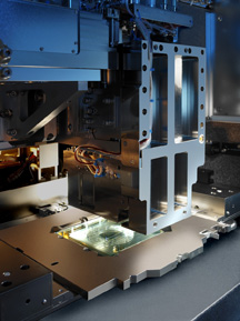
Teron 600 at work inspecting a reticle with 193nm light. The large NA objective is visible below the 6” square mask (source: KLA-Tencor).
There are now three plausible lithography paradigms for the 2Xnm generation: EUV, pitch-splitting double patterning (PSDP) with immersion 193nm exposure, and wet 193nm with source-mask optimization (SMO) and other tricks. Thus it is not enough to inspect reticles with the same actinic wavelength as today’s immersion scanners. Additional defect categories must be detected and complex wafer-plane modeling adopted to evaluate their impact, according to Lopez. The Teron 600 platform (see figure) is thus intended to detect defects on all types reticles proposed for the 2Xnm generation, whether they will be printed with transmitted 193nm or reflected EUV radiation, and is designed to be extendable for future shrinks.
Other reticle defect inspection tools have employed sub-200nm radiation, but not in the same way as the industry-standard 257nm tools. In particular, the Applied Materials Aera2 and Zeiss AIMS systems have emulated the excimer illumination and reticle-side numerical aperture of exposure tools, while projecting an enlarged wafer-like image for analysis. Anomalies in that image directly relate to defects that appear on a developed chip, but do not indicate what caused those anomalies. The Teron 600 (and KLA-Tencor’s TeraScan systems) image the photomask with a high numerical aperture objective in transmission and reflection to capture the structure of the photomask at maximum possible resolution, finding numerous anomalies, many of them too subtle to affect wafer CD.
Photomasks no longer look like the target wafer patterns. For the 3Xnm and 2Xnm nodes, computational lithography techniques such as Inverse Lithography Technology (ILT) and Source Mask Optimization (SMO) produce fractured geometries with an enormous number of very small features, making the masks difficult to manufacture. In PSDP, not all the edges that define the CDs of a circuit layer are on a single mask, necessitating multilevel database processing and context sensitive defect detection to deal with “mask to mask” (M2M) defectivity. To reject the nuisance defects, the Teron 600 employs computational lithography methods in real time to simulate the pattern at the wafer plane. Resist response and – for SMO – the complex programmed illumination distributions must be included in the model in order to correctly evaluate the yield impact of detected anomalies. If the computation indicates that an anomaly is likely to cause an unacceptable CD excursion, reticle plane images are available to suggest repair strategies to the user.
“EUV reticle inspection is actually the most straight forward,” claimed Lopez. “The key requirements are high resolution inspection in the reflection mode and low-noise imaging in an ultra-clean environment.” With a 55nm pixel size, the capability of finding programmed defects in multilayer reflector topography down to 2nm height and <40nm diameter and to model EUV illumination effects, the Teron 600 is ready for first-generation EUV reticles, claimed Lopez. Low noise results from the use of an innovative, quasi-CW 193nm laser system. Lopez reported that KLA-Tencor has more than 10 lasers from its secret overseas supplier, and some have operated for 2 years in the lab.
The Teron and TeraScan platforms are compatible, facilitating a mix-and-match capacity optimization strategy and effective integration of data from critical and non-critical layers, according to KLA-Tencor. The Teron 600 is reported to have successfully inspected 30 highly secret prototype reticles created for source-mask optimization / inverse lithography technology, double-patterning lithography, and EUV (both patterned masks and blanks). The tool comes in two configurations, depending on whether the user wants a 3- or 4-hour turn around time for inspection. The first beta test tool is being shipped now, leaving 4 more being tested at the KLA site. Lopez estimates that roughly 10 high-end mask shops will need the Teron 600 for near term development. Since it can be applied to all projection lithography reticles currently being investigated, no technology commitment need be made, except, perhaps, not to emphasize imprint lithography. – M.D.L.
Tags: 193nm, 22nm, 32nm, EUV, IC, inspection, litho, mask, reticle, SMO
