Thursday, October 22nd, 2009
If EUV lithography is to succeed, infrastructure gaps will need to be addressed forthwith. The lack of inspection tools for EUV masks and substrates constitutes one such gap, now recognized as a priority by SEMATECH. At the OSA/APS Frontiers in Optics (FiO) meeting held in San Jose, October 11-15, Carmen Menoni of Colorado State University and an international team of co-authors showed how one key actinic mask inspection task might be accomplished.
The enabler for actinic inspection, according to Dr. Menoni, is a high-brightness EUV radiation source that is more convenient than the ones developed for lithography. The source presented at the FiO meeting was a table-top EUV laser at 13.2nm that uses a highly ionized (Ni-like) cadmium plasma to produce a beam with 2 microW of average power. That wavelength is close enough to the 13.5nm peak reflectivity of the multilayer stack of an EUV mask substrate to facilitate at-wavelength inspection.
The laser light goes into a simple EUV microscope where a Fresnel zone plate acts as a condenser lens to illuminate a test mask in just the way it would be in an EUVL scanner. The light reflected at a 6 degree angle is then projected and magnified by an off-axis zone plate objective with 0.06225 numerical aperture (NA) onto a CCD detector array.
 With such a low NA, the zone plate resolution might not seem useful for defect inspection, but the objective has ¼ the numerical aperture expected for the first generation EUV exposure tools, which will have 4x demagnification. Thus, the image at the CCD is a magnified version of what would be exposing a wafer. Any anomalies in that image would correspond to printable mask defects. The optics train of the simple laser microscope is just what would be needed for a prototype EUV AIMS tool, the gold standard for mask inspection.
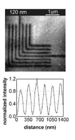
Initial results showed 55nm resolution in the mask plane, which would correspond to 14nm resolution at the wafer. Exposure time on 5m square nested elbow targets (see figure), however, was 20 sec and the initial images were degraded by laser speckle. Vibrating the condenser plate and averaging over 90 seconds produced higher quality images that might reveal subtle defects through die-to-database comparison.
The most remarkable feature of the system was that it all really did fit on a (rather large) table top and did not require a building sized synchrotron to function. Other talks at the meeting described improvements in extreme UV lasers. In particular, another Colorado State group described an all-diode-laser pumped soft X-ray laser at 18.9nm. If the efficient diode-pumped laser technology can be used with Ni-like Cd, much higher average power can be expected, leading to faster AIMS defect review. – M.D.L.
