Monday, March 22nd, 2010
The upcoming Spring Materials Research Society (MRS) Meeting in San Francisco will feature a separate “Nanocontact and Nanointerconnects Workshop” to explore the biggest secret about the smallest devices: for the near-term there’s nothing better than standard metal. The workshop will address both theoretical and experimental approaches to formation, carrier transport, and reliability, and so will also explore the long-term potential for novel materials and structures.
Whether it’s a quantum dot for memory, a self-assembled molecule for a switch, or a carbon-nanotube (CNT) sensor, it needs electrical connections for power and signals. As new materials with novel composition and geometry are explored, the underlying physics of contact/interconnect formation and carrier transport needs to be re-examined.
The scheduled speakers for the all-day event are as follows:
- Stan Williams, HP Labs (plenary), Palo Alto, USA
- Paul S. Ho, University of Texas, Austin, USA
- Suzanne Mohney, Penn State University, USA
- Francois Leonard, Sandia National Labs, USA
- Juan Jose Palacios, Universidad de Alicante, Spain
- Richard Martel, University of Montreal, Canada
- Jon Pelz, Ohio State University, USA
- Ingann Chen, National Cheng Kung University, Taiwan
- Hanno H. Weitering, University of Tennessee/Oakridge National Lab, USA
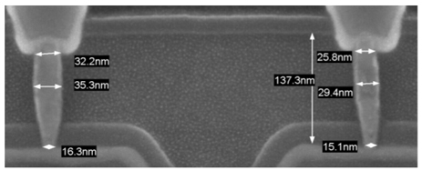
In the real world of high volume manufacturing (HVM) of nanoscale devices, the performance is typically gated by the interconnect. The speed of the switch is now generally faster than the time needed to get electrons to flow down the wire to the switch. The resolution of the sensor array is now limited by the shadows from the wires. Converting a signal between electrons and photons—using detectors and laser diodes—adds unacceptable delay. No one has found a room-temperature superconductor, and after decades of research there is not even a hint that one could exist. In all, there’s nothing better than a 15nm copper contact (see figure).

SEM cross section of 15-16 nm Cu contacts post-anneal. There is no Cu diffusion through the Ru to the silicide, and no void formation. (source: IBM)
Just over two years ago at IEDM 2007 in Washington, D.C., an evening panel discussed “Looking beyond silicon – a pipe dream or the inevitable next step?” While most of the discussion had focused upon so-called “More than Moore” devices (beyond silicon-based CMOS), one of the final conclusions was that interconnects appear to be our real limitation. “There is no new switch in sight,” said Wilfried Haensch, IBM senior research manager. “All candidates are either non-manufacturable or they can not be wired up.”
So, any proposed new nanodevice must outperform CMOS, and for the near-term must rely upon the same connections as available to standard silicon CMOS. As the International Technology Roadmap for Semiconductors (ITRS) 2009 edition’s Emerging Research Devices (ERD) section mentions on page 23, “An accelerator that is offered as a CMOS replacement should offer a performance improvement relative to its CMOS implementation of an order of magnitude.” To justify the R&D costs and integration risks, any new conductor technology would likewise probably have to provide an order of magnitude improvement in performance.
Christopher Case, ITRS Interconnect TWIG Chair (currently with Solid State Solutions), writes in the January 2010 issue of Future Fab (special ITRS issue) that Cu is expected to be our interconnect for at least the next 15 years. For any interconnect to complete with nanoscale copper contacts, Case reminds us that, “the goal is propagating terabits/second at femtojoules/bit.” He provides an excellent overview of the inherent challenges in trying to improve upon copper contacts.
As Case reminds us, from first principles of materials it seems that the only way to improve upon today’s copper contacts is to eliminate the internal grain boundaries that induce electron scattering. We can grow CNTs or single-crystal metal fibers from nanoscale catalyst dots, but we’re still only at the proof-of-concept stage. We’ve discovered graphene, but we’re still just beginning to learn about what we have yet to prove. If you attend the MRS Nanocontacts and Nanointerconnects Workshop in two weeks, you’ll probably learn the lower size limits of what we can build today and most of tomorrow.—E.K.
Tags: 22nm, CMOS, CNT, Cu, FET, FPD, IC, memory, MEMS, nano, PV, R&D
