Friday, February 25th, 2011
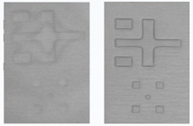
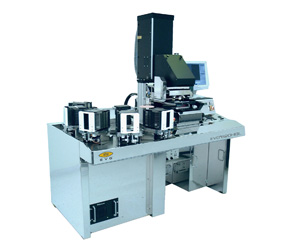
After successful high-volume manufacturing (HVM) beta-site evaluations, EV Group (EVG) has released an automated mask aligner fine-tuned to maximize yield in high-brightness LED (HB-LED) fabs. The EVG620HBL upgrade to the 620-platform creates an automated tool that can align and expose 165 wafers/hour, with new illumination optics that can easily see alignment marks on the transparent sapphire substrates commonly used for GaN-epi today (figure). New to this tool are five cassette stations – significantly more than competitive offerings – to enable continuous fabrication of devices at up to 220 wafers per hour in first print mode for substrates up to 150mm diameter.

HB-LED GaN-epi on sapphire alignment marks, (LEFT) with conventional illumination, and (RIGHT) with new illumination in EVG620HBL tool. (source: EV Group)
EVG claims that its bonders and mask aligners are being deployed by four of the top five major HB-LED manufacturers, and that customers drove the creation of the 620HBL to increase their line yields and throughputs. Since the next major market for HB-LEDs is general lighting, cost reductions in high-volume manufacturing (HVM) are critical if CFLs and other general purpose lighting technologies are to be replaced. Throughput is critical for overall cost-reduction, to be sure, but yield losses probably dominate cost-of-ownership (CoO) considerations in evaluating competing fab tools.
Typical HB-LED process flows include 4-5 mask steps, and misalignment between masks is a major factor in yield loss. This new aligner now includes special recipe-controlled microscopes with illumination spectra and polarization optimized for pattern contrast with various wafer and layer materials. It is dedicated to high-brightness LED on sapphire, but it can be used equally well with other substrates such as silicon carbide (SiC), aluminum nitride (AlN), other ceramics, or even metal.
Basic tool capabilities include the following:
- Wafer diameters: 50-150 mm, changeable in <1 minute
- Substrates: Sapphire, SiC, Si, AlN, metal, ceramic
- Throughput: max.165 wph (aligned), 220 wph (first print)
- Top Side Live Alignment Accuracy: +/- 1.0 micron
- Bottom Side Alignment (option): +/- 1.5 micron
- Exposure: Proximity, Soft-, Hard- and Vacuum-contact
- Pattern resolution: 2.0 micron (Proximity)
- Footprint: 2.1 m2 (figure)
- SECS II/GEM interface : optional
“Just last month, one of the leading HB-LED manufacturers ordered an EVG560HBL bonder,” stated Paul Lindner, EVG’s executive technology director, “and the EVG620HBL is the latest result of our ongoing efforts around enabling HB-LED manufacturers to develop more efficient, cost-effective and higher yielding devices to meet their customers’ demands. We look forward to making further inroads with this latest offering, which also features high-accuracy handling and alignment of fragile or warped wafers.”
In an exclusive interview with BetaSights, Thomas Uhrmann, EVG’s business development manager, explained how the quick-swap (<1 min.) vacuum chucks allows for HVM compensation of the different inherent bows of different epi-wafers. Though the tool can function in contact- and vacuum-modes, proximity-alignment of tens of microns is almost always used to extend mask life and reduce particles in patterning HB-LEDs.
For 150mm-diameter sapphire wafers, the thickness spec. today is 1.0-1.3mm. However, once GaN epi-layers are grown using MOCVD, the mismatch between substrate and epi Coefficients of Thermal Expansion (CTE) always induces stress and warp. A typical process flow to grow the epi stack involves several hours at ~700°C to grow the buffer layers, followed by ramp to ~1050°C to grow the multi-quantum well (MQW) and p-GaN layers. As the wafer is heated and then cooled, the CTW-mismatch first creates compression and then tension in the epi layers. EVG’s applications engineers reportedly see up to a full 1 mm of warpage in GaN-epi on sapphire wafers at room temperature.
Since an LED’s color is determined by the composition of the epi-layers, and since different epi-layers with have different CTEs, epi-wafers to produce different LED colors will have different extents of bow. Consequently, a HVM LED fab can use this new tool with a different chuck for each product to ensure optimal wafer flatness during proximity alignment.
There seems to be one big variable in the world of GaN-epi growth: the possibility of homo-epitaxy on GaN substrates. Since control of defects is critical for GaN device functioning, and since hetero-epitaxy always induces defects, going to homo-epitaxy offers inherently superior device performance. The ability to use simple back-contacts saves fab costs, too. If UCSB spin-out Inlustra Technologies can ramp up 50mm diameter GaN substrates and offer them at reasonable prices this year, then sapphire might start to give way as the substrate of choice for HB-LED HVM. However, since GaN is itself rather transparent, the new EVG aligner seems like an ideal tool for HB-LED patterning. -E.K.

