Friday, January 7th, 2011
IEDM 2010 provided extensive details of the near term evolution of mainstream IC memory technologies DRAM and NAND Flash. There were many other presentation on up-and-coming memories like phase-change memory (PCM) and resistive random access memory (ReRAM), but the relative newcomers are struggling to keep up with the moving targets in DRAM and Flash performance/cost capabilities.
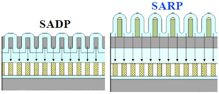
Samsung uses Self-Aligned Reverse Patterning (SARP) for 2Xnm node Flash chips (source: IEDM2010, S05P01)
Samsung researchers showed (S05P01) how evolutions of 3Xnm node NAND Flash processing can be made to work for 2Xnm node chips, and claimed that variability can be managed with lithography and annealing/oxidation to allow for 3-bits per cell. Sidewall spacer double-patterning (SSDP) will be used for 2Xnm half-pitch structures, but in a variation Samsung terms “Self-Aligned Reverse Patterning” (SARP) where the sidewalls define the pattern instead of the cores/spaces (figure). The CD uniformity of SARP is reportedly <5%, compared to >10% when trying to use the cores/spaces of “SADP,” and the improved uniformity reduces threshold voltage (Vth) distribution. An unexplained “novel tunnel oxidation” process was used to concentrate the implanted boron (B) near the silicon surface, resulting in a ~0.5V increase in the initial Vth along with lower junction leakage characteristics.
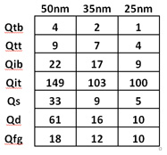 Intel/Micron researchers presented on (S05P02) “25nm MLC NAND Technology and Scaling Challenges,” showing a 64Gb multi-level cell (MLC) NAND with a cell size of just .0028um2, and with only 30-40 electrons separating logic-levels. Wordline material is not specified but is patterned using a subtractive flow. The number of electrons needed to induce a 100mV shift in Vt scales with reducing material volume, and electrons trapped in parasitic locations can be easily detrapped to show up as a charge loss mechanism. At the 25nm node, just a single electron at the wrong location can induce a 100mV shift (table)!
In nanoscale transistors the conduction through the channel is essentially filamentary, and the interaction of dopant atoms and interface states or traps causes channel conduction to be non-uniform. At 25nm, there are ~75 boron atoms/cell (with 50-100 as the +-3sigma range), and the Vt is expected to vary by ~30% purely due to random dopant fluctuation. In addition, noise is caused by a variable number of electrons tunneling–due to quantum mechanical effects–during each programming pulse, and since the number of electrons is reduced with scaling this random noise increases.
Circuitry tricks like the use of error-correction control (ECC) bits has been used to compensate for noisy memory cells, but as noise increases the number of ECC bits must also increase. At 25nm the circuit uses a 1KB codeword. However, there is a limit to the present ECC approach, and new algorithms may be needed.
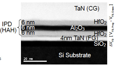
TEM cross-section of a Flash memory cell showing ~4nm TaN floating-gate (FG) and hafnia-alumina-hafnia (HAH) inter-poly dielectric (IPD). (source: IEDM2010, S05P03)
Researchers from North Carolina State University (NCSU) working for Intel and the National Science Foundation (NSF) presented (S05P03) on the scaling limits of Flash memory cells. By properly engineering sandwiches of Hf-based high-k dielectrics in combination with TaN metal floating- and control-gates, scaling down to 1Xnm node was shown. Replacing the conventional oxide-nitride-oxide (ONO) dielectric stack with HfO2-Al2O3– HfO2 (HAH) (figure) or a single layer of HfAlO for the inter-poly-dielectric (IPD) lower band offsets and reduce gate-to-gate leakage.
A single layer of HfO2 crystallizes during the 450°C floating-gate anneal (FGA) such that grain-boundaries form to provide leakage paths. The alumina in the middle of the HAH stack remains amorphous post-FGA, so leakage was comparable to the HfAlO. However, Fowler-Nordheim modeling predicts that the electron tunneling distance for HAH will be longer than HaAlO for the same physical thickness, so leakage should be reduced using the stack.
Process Flow:
-
n-Si substrate
-
Tunnel ox by furnace (7nm SiO2),
-
FG by PVD (10nm TaN),
-
IPD by ALD,
-
CG by PVD (10nm TaN).
Scaling of the TaN FG (tried 10nm, 4nm, and 1nm) while maintaining the same HAH IPD. Program-erase characteristics shown well down to 1nm thickness! Endurance tests showed no changes from 10nm to 4nm, but 1nm showed Vfb shift while the PE characteristics were maintained.
eDRAM for 3Xnm node ICs
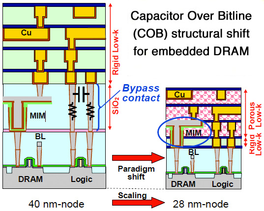
Renesas' capacitor in porous low-k (CAPL) eliminates W bypass contacts for reduced eDRAM delay (source: IEDM2010, S33P03)
Renesas researchers presented (S33P03) on, “A novel cylinder-type MIM Capacitor in Porous Low-k Film (CAPL) for Embedded DRAM with Advanced CMOS Logic.” A paradigm shift is occurring for embedded DRAM (eDRAM) using traditional capacitor over bitline (COB) structures: the tungsten (W) bypass contacts (BCT) to transistors where there are no metal-insulator-metal (MIM) cylinders (figure) now induce excessive circuit delays. The BCT induced delay has been simulated to slow down the circuit by ~10% in 4Xnm node circuits, and the delay only increases in 3Xnm node structures. To avoid the bypass contacts, the MIM cylinder could be built into the interconnect layers, but would be challenged by the pores of advanced low-k dielectrics used in interconnects today.
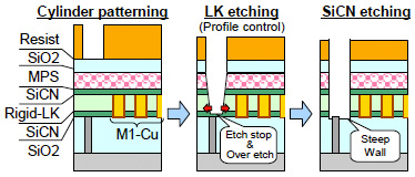
Renesas' capacitor in porous low-k (CAPL) eDRAM structure requires careful control of the etch process to provide smooth sidewalls with a bottom angle of ~88° for void-free filling. (source: IEDM2010, S33P03)
Using SiOCH molecular pore stacking (MPS) low-k dielectrics with average pore size of 0.4nm as part of the interconnect, the etch process must be carefully tuned to provide smoothly tapered sidewalls (figure). Low-k films with larger pore sizes allowed for metal precursor penetration into the dielectric with serious performance degradation, while 0.4nm pores could withstand exposure to a Ti precursor for a ”surface-reaction controlled CVD” process (pseudo-ALD) followed by NH3 exposure to form TiN as the bottom electrode. Then so-called “CVD” of ZrO2 and TiN completes the MIM structures, with capacitances reportedly ~8 fF/cell. Capacitance ~11fF/cell could be realized by extending the CAPL structures up through an additional metalization layer at the same pitch (~40 nm MIM pitch @ 3Xnm node). Reliability of the MPS has been characterized, including a Vbd of ~2.7 V which is greater than the operating voltage.
So eDRAM technology—like stand-alone DRAM—can be extended to smaller geometries by the use of ALD to provide conformality in forming MIM stacks inside of extremely high aspect-ratio (AR) structures. Before deep-trench DRAM was killed a while back, up to 80:1 AR structures had been proven as manufacturable using ALD. So, it looks as if the industry workhorse memory that is DRAM is still extendable to 2Xnm nodes and perhaps beyond, while NAND Flash looks good down to 12nm geometries. Other memory technologies will probably remain relegated to niches for the near term. E.K.
Tags: 12nm, 16nm, 22nm, 25nm, 2Xnm, 32nm, 3Xnm, ALD, COB, Cu, DRAM, eDRAM, Flash, HfO2, IC, IEDM, Intel, Micron, MLC, MPS, NAND, PCM, Renesas, ReRAM, Samsung, SARP, W
