Monday, February 23rd, 2009
JEOL will install the first e-beam direct-write-on-wafer (EBDW) lithography tool to support nanotechnology development in the Pacific Northwest when the University of Washington takes delivery of a JBX-6300FS tool. The system will be installed in the state-funded Washington Technology Center Microfabrication Lab. Funding for the tool acquisition was provided through a state-supported STAR researchers’ grant to Michael Hochberg, Assistant Professor of Electrical Engineering, and a matching grant from the Washington Research Foundation.
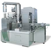
 In addition to Professor Hochberg’s work in nanophotonics, this tool (see figure) will support nanoscience research throughout the University of Washington and the region. The tool will be available to students as well as researchers from several outside companies whose work includes MEMS research and production/process development. The WTC is the only facility of its type in the Pacific Northwest, offering a publicly-accessible clean room and offering hands on R&D and training support.
This model is capable of writing line widths down to 8nm on substrates up to 200mm in diameter. It is a spot beam, vector scan, step and repeat tool for small volume production as well as “sandbox lithography.” It is also targeted at nano-imprint lithography (NIL) 1:1 mold making, which seems to be gaining in popularity judging from the presentations at SPIE this year. “This is the most flexible, capable machine that you would buy to build nanostructures,” enthused Hochberg.
This new tool joins the one installed n 2007 at the University of Santa Barbara Nanofabrication facility, which is part of the National Nanotechnology Infrastructure Network of the National Science Foundation. There, the going rate is $150 (acedemics) to $450 (industry) per hour for e-beam litho use. They have a wide range of other process tools, and even say they can run the tools for you. –E.K.
Tags: 32nm, 45nm, EbDR, IC, lithography, MEMS, NIL, node, R&D
