Tuesday, January 6th, 2009
The first issue of the BetaSights Newsletter has been published (see link to a free copy in the right-side column of this page under “Newsletters”), and a reader has already provided a correction. Michael Current (San Jose, California) noticed that the initial web-link to the slides from Prof. Asenov’s IEDM 2008 variability presentation was incorrect; the correct address is http://www.elec.gla.ac.uk/groups/dev_mod/presentations/Asenov_IEDM_08.pdf to access all 25MB of in-depth information.
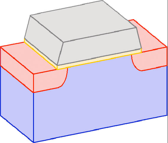
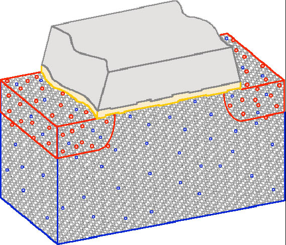
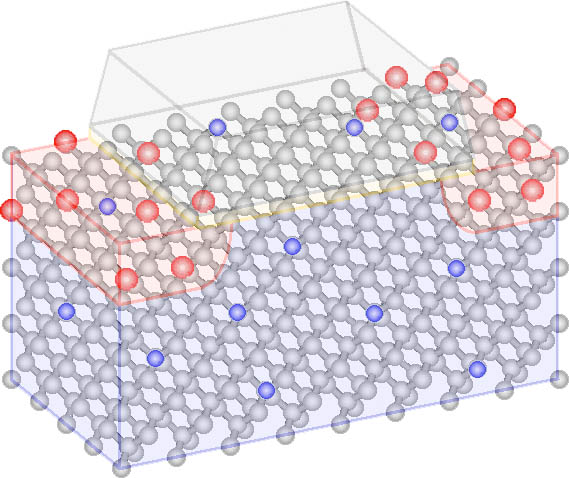
 As Current commented about this presentation, it is rare to find a set of slides that so thoroughly explores the leading-edge of fab technology, and even more rare to find a set that does so without obtuse mathematical equations. For example, slide #6 in this set shows three images for MOSFET transistors (see Figures to the right): the top for a modeled ideal transistor, the middle for a 22nm node device, and the bottom for a 4.2nm MOSFET. You can clearly see the granularity of matter at 22nm, which explains why statistical variability is inherent at this scale.
 Looking at the 4.2nm rendering, everything is so chunky that it’s difficult to even try to draw a line to define where one region ends and another begins. At the risk of getting philosophical, even concepts like “junction” or “barrier” seem to lose meaning at this scale. Chips need to operate near room temperature where there is sufficient energy (ekT) to make things move around, but even if atoms didn’t diffuse (in a hypothetical alternate universe) it still seems impossible to extend current fab technologies to make devices this small.
 Though we may have seen the limits to CMOS shrinks, some of us still want to move to 32nm and 22nm node processing. People are contemplating these moves with an understanding that new ways of working will be needed. As Asenov concludes, “Statistical variability demands a statistical approach to design and will force fundamental changes in the design paradigm.” –E.K.
