Wednesday, February 25th, 2009
Applied Materials’ Technical Symposium at SPIE 2009 featured a panel discussion on next generation lithography (NGL) that was moderated by the company’s Ken MacWIlliams. The outstanding panelists were C. Grant Willson (UT-Austin), Burn Lin (TSMC), Jongwook Kye (AMD), Steve Radigan (Sandisk), and Milind Weling (Cadence). As would be expected from this panel, EUV steppers were not expected to be used prior to 2012. “EUV has gone from if to when to if again,” commented Weling.

Kye reminded attendees that 2012 is just three years from now, and lacking any fab data from which to extract design rules there is no way that designers can plan for chips to be made with EUV. Perhaps by 2015. Of the various options for double-patterning (DP) lithography, Kye sees litho-etch-litho-etch (LELE) as too expensive for mainstream production, so the industry needs to pursue litho-freeze-litho-etch (LFLE) or sidewall-spacer DP (SSDP).
Willson, patterning pundit, commented that for about $100M you can have one EUV tool, or 10 NIL tools sold by his current company, Molecular Imprints. He feels that NIL has the best chance of patterning 22nm features, but acknowledges that mold defect concerns cause hesitation in commiting the technology to production. The many presentations on NIL integration at SPIE this year may have finally cleared the emotional fear that this is just fancy contact printing, so now perhaps someone will try this in an IC fab to get the real defectivity numbers.
Lin promoted bold new ideas in multi-beam direct write and DP. If MEMS technology can produce dense arrays of electron emitters, and said emitters can be stepped or scanned across a field then e-beam could be cost-effective for all critical layers on a chip. For DP, he showed a high-level concept of a scanner to simultaneously expose two masks side-by-side and through optics combine the images into a single pattern.
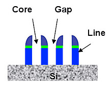
Regarding the cost of various DP schemes, if your design is for regular memory circuits or logic with gridded-design-rules (GDR) then all of the depositions and etches needed to integrate sidewall-spacer DP (SSDP is a patented variation of self-aligned DP or SADP) are expected to add approximately US$5 to cost per layer. Additional details of Applied Materials’ SSDP flow as detailed by project leader Chris Bencher will be in the next issue of the BetaSights Newsletter. –E.K.
