Thursday, April 2nd, 2009
The control of complex interdependencies is critical for the successful manufacturing of nanometer-scale ICs. Every aspect of every unit process step in the line must be ever more tightly controlled to ensure that 45nm and 32nm node chips can be made with good yield. To serve the market, Novellus continues to announce new integrated surface-treatment and deposition process-sets for dielectrics (Ref: BetaBlog 2009 March 20, and BetaSights Newsletter 2009 March 24), this time for barrier layers as thin as 10nm.

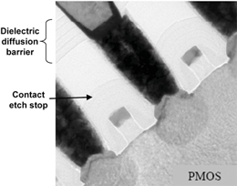
TEM cross section of a 65nm node device showing diffusion barrier and contact etch stop formed by multi-station sequential deposition (source: Intel)
The standard dielectric barrier material for 90nm and 65nm node interconnects has been nitrogen-doped silicon carbide (SiCN) with dielectric constant (k) of ~5. When integrated with a standard SiCO film of k~2.7, a SiCN barrier results in a k-effective of ~3.3 for the final stack. To reach a target k-effective of ~3.0, there are two basic approaches: lower the k value of the barrier with a new material, or else thin the barrier with the same material. A new material requires new integration work, so it is easier to stay with SiCN if it can be done. Novellus has shown that the laminate/multi-layer films (see etch decorated layers in figure) deposited in multi-station sequential processing (MSSP) tools can meet barrier specs despite less mass per area.
Taking advantage of interface and bulk film controls afforded by MSSP, Novellus researchers have successfully demonstrated that 25nm SICN can replace 50nm of the barrier material. “Novellus’ diffusion barrier films meet today’s performance needs and have been demonstrated to meet the EM and dielectric breakdown requirements for future technology generations,” said Kevin Jennings, senior vice president and general manager of the PECVD business unit. The company claims that the line-to-line leakage (extacted at 2MV/cm) was essentially identical at the bottom of the instrument detection limit for stacks using the SiCN barrier at thicknesses of 70, 50, and 10 nm.
“Thinning dielectric barriers is an approach that has been used by several IC manufacturers in the 65-45nm transition,” explained Mandayam Sriram, Director of Technology for PECVD. “This approach for sub-45nm technology nodes is challenging and alternate approaches are being considered. We now have a viable, demonstrated HVM solution for sub-45nm technology nodes with the low risk, thinner barriers that provide the RC scaling requirements and at the same time meet the EM and TDDB requirements.” More exclusive comments from Sriram about dielectric integration will be in the next BetaSights Newsletter. –E.K.
Tags: 32nm, 45nm, 65nm, barrier, CVD, IC, low-k, PECVD, SiCN
