Friday, March 20th, 2009
Novellus’ applications labs have been working on CVD low-k dielectrics targeting 32nm node multilevel metal specs, and the result is “dense” ultra-low-k (ULK) film with bulk k=2.5 and the potential to go lower. Combined with the company’s multi-station sequential processing (MSSP) tool architecture for the barrier/cap depositions and UV/thermal cure steps, the result is a claimed 5% reduction in the effective k compared to porous low-k (PLK) films. With complex interdependent trade-offs in interconnect materials today, there are inherent complexities in the solutions as well as in the descriptions of those solutions. To discuss such complexities, instead of a one-time press release the company has launched a new technology information page on online.
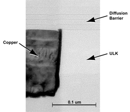
Despite mis-directions from early editions of the ITRS, in which a new low-k material was supposed to be integrated into production for each new node, the world has mostly settled on the use of CVD SIOC(H) for k~3 films. To be sure, successively lower capacitances would have nicely lowered the RC delay factor in interconnects, but new materials have been difficult to find and expensive to integrate. In particular, dielectric barrier and etch-stop layers require relatively higher k value such that the effective k for the whole dielectric stack (see figure) is always greater than that for the main low-k film alone. “RC scaling is about k-effective, not the absolute k value of each layer,” reminded Mandyam Sriram, director of technology for Novellus’ PECVD business unit.
“We don’t think that it’s important to compete on the marquee value of bulk low-k. We’ve taken a different approach,” said Tim Archer, executive vice president of the PECVD business unit, in an exclusive interview with BetaSights. “Most of our competitors have been working on PLK in the 2.3-2.4 range. We think that we can deliver a full stack that will rival or beat the k-effective of the PLK.” The barrier layer depositions and UV cure steps really can make or break k-effective.
The company’s “dense” ULK film is reportedly deposited as a single phase from a single precursor, instead of the two precursors used for PLK deposition. Still, the ULK material requires a cure step that outgases some material, and data shows the material’s k value reducing along with density. The company officially has no comment on comparisons between its ULK and the molecular pore stack (MPS) ULK shown by NEC (Ref: BetaBlog 090317). More exclusive info on low-k dielectric integration and Novellus’ plans will be in the next BetaSights Newsletter. –E.K.

