Tuesday, March 17th, 2009
Breaking news about a leading porous low-k (PLK) material from Japan was first revealed in the SemiNeedle Planarization Lounge Forums (www.semineedle.com/forums/5001) about two months ago. During an expert panel discussion on CMP integration with low-k materials (moderated by this editor, summarized in “Chemical-Mechanical Planarization (CMP) technology consensus 09Q1” publication available at the site), Dick James, of reverse-engineering expert firm ChipWorks, disclosed that he had recently seen the first use of a PLK in a commercial chip his company had examined. Fujitsu is now fabbing Via Technologies’ new Nano CPU for “surfbored” (joke spelling intentional) notebooks, using nano-clustering silica (NCS) PLK of k~2.3.

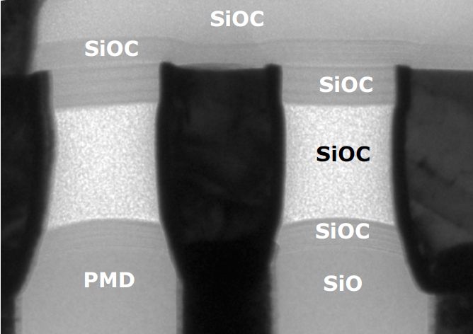
Via Technologies Nano CPU interconnect cross-section, fabbed by Fujitsu, showing use of NCS porous SiOC between caps of dense SiOC (source: ChipWorks)
There are many known integration challenges with PLK materials: material degradation during plasma etch, pore-sealing on sidewalls, compatibility with metal CMP processes, etc. In particular, for CMP most workable integrations use a capping layer of another dielectric such as standard CVD SiOC or a spin-on undoped silicate glass (USG). The Via Nano chip fabbed by Fujitsu shows NCS capped with a layer of CVD SiOC according to ChipWorks (see figure).
In Session 26.7 of IEDM2008, NEC showed “damage-less” full Molecular Pore Stack (MPS) SiOCH intermetal dielectric integration including direct CMP. MPS thin films are formed from ring-type siloxanes (with high carbon content) in CVD chambers, resulting in dielectric k=2.5 and resistance to plasma-induced damage. With small average pore size (<1 nm) there is low potential for water-absorption with MPS films, and having smaller pores reduces intrinsic line edge roughness (LER).
The bulk MPS material is hydrophobic so that an aqueous process like CMP leaves water marks behind. NEC experimented with He plasma treatment to alter the MPS surface, and found that 15 seconds reduces carbon to make the surface hydrophillic, but treatment for >30 seconds tends to form a top crust which cracks and shows as scratches. Using a He-plasma treatment in the 15-20 seconds range is thus key to cost-effective integration of MPS in dual-damascene Cu flows. The company claims that there is margin for overpressure in CMP using this dielectric without a cap. Full details about these development are in the latest BetaSights Newsletter. –E.K.
Tags: cap, CMP, dielectric, IC, interconnect, low-k, MPS, NCS
