Friday, January 22nd, 2010
The IEEE’s International Electron Devices Meeting (IEDM) is still the place to see the latest micro- and nano-electronics research targeting commercial markets. On December 8, 2009, French researchers from Leti/Minatec showed “3D sequential CMOS integration” as <600°C processing of PFETs using a (110) orientation FDSOI layer that was transferred on top of NFETs made using traditional (100) orientation wafers. A decrease by 4Å of the PFET Equivalent Oxide Thickness (EOT) is measured using the <600°C process. Electrostatic coupling between stacked FETs is demonstrated, enabling 22nm node SRAM stabilization through a 130mV dynamic shift of threshold voltage.
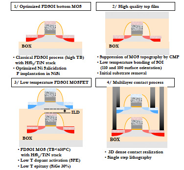
With complimentary metal-oxide semiconductor (CMOS) devices now shrunk down to 32nm scale in production, and 22nm in development, the industry has done almost all that can be done in 2D. Thus, the motivation to explore the 3rd dimension, and the interest in finFETs (3D transistor structures) and through-silicon vias (TSV for 3D stacks of circuits). TSV are used to connect together two or more silicon IC layers that were independently fabricated in parallel. This exciting new work from Leti connects together two silicon IC layer that are fabricated sequentially (figure).
 Most of the fundamental unit process steps needed to do this work seem to have been known in prior art, but no one had combined everything together to create such a novel circuit structure. Previous work by Tracit (now part of Soitec) had shown the possibility of doing thin-film transfers of silicon from one wafer to another with structures beyond blanket layers. From first principles of materials engineering, dopants can provide grain-boundary “pinning” that slows grain growth during thermal exposure. Relatively rapid SiGe epitaxial growth at <600°C has been shown.
The bottom NFET layer of transistors use a 5mn HfO2 and TiN/Poly-Si(N+doped) gate stack. Raised source/drain (RSD) structures were formed by salicidation of Ni, then an innovative fluorine implant step stabilizes the NiSi such that it can withstand the thermal budget of the top PFET processing to come. The sheet resistance of the NiSi(F) blanket film is 12-14 Ohms-square as formed and after the thermal budget exposure of top layer processing. Deposition of the thin Inter Layer Dielectric (ILD) followed by CMP to eliminate topography, provides the surface for the 200°C molecular bonding of a SOI substrate as a perfect quality top active layer.
Top MOSFETs are then processed with an overall thermal budget limited to 600°C:
• HfO2 anneal 515°C (5 min),
• Poly deposition 515° (40 min),
• Spacers deposition 480°C (time not specified), and
• SPE dopant activation 600°C (2 min).
In addition to Solid Phase Epitaxy (SPE) for dopant activation, this flow uses SiGe epitaxy at 600°C to form RSD. For 30% Ge, 4nm/min growth rate has been obtained. To optimize the PMOS layer (above the NMOS), in situ B-doped SiGe RSD were also tested.
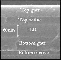
 Functioning circuits have been created using this approach, including an equilibrated inverter with (110) PFETs on top of (100) NFETs, and a 3D SRAM with (100) load PFETs stacked on (100) drive and access NFETs. The unique 3D electrostatic coupling between layers was quantified depending on the targeted ILD thickness: for 120nm thin ILD the top transistors can be considered as FDSOI with thick BOX, while for 60nm ultra-thin ILD the result is a Double Gate like device (figure). In the latter case, a 130mV threshold-voltage shift is observed when the top NFET lies above a bottom transistor, demonstrating that the threshold voltage of top FETs can be dynamically tuned by biasing bottom FETs so as to stabilize SRAM cells.
This work shows that there are many ways to go “3D” with ICs. By stacking layers closely together, we achieve a new degree of freedom in circuitry: dual-gate devices when needed, or double the number of transistors per unit area of silicon. Compared to parallel integration using TSV, sequential integration provides unbeatable results in one basis parameter: overlay error. Layer-to-layer alignment using TSV generally targets ~500nm, while this manner of stacking allows for ~10nm precision! –E.K.
Tags: 22nm, 3D, dual-gate, epitaxy, FDSOI, FET, finFET, HfO2, HK, IC, NiSi, R&D, RSD, selective epi, SiGe, SPE, stack, TSV
