Tuesday, January 13th, 2009
At SEMI’s Industry Strategy Symposium (ISS) running at Half Moon Bay, California today, IMEC president and CEO Gilbert Declerck talked about the need for R&D to facilitate IC industry growth. An industry based on answering the question, “what have you done for me lately?” can never rest on past successes and must continue to innovate. Even in difficult economic times, major technology investments are needed to keep up with evolving customer expectations. IMEC’s “open innovation” R&D model has resulted in the organization being able to show electrically functional 0.186µm2 32nm SRAM cells using EUV for contact hole patterning.
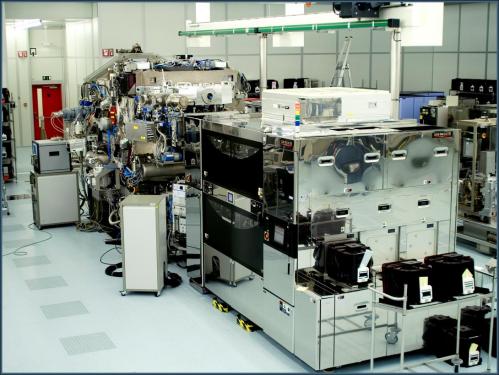
The two ASML EUV full-field tools delivered to IMEC and Albany Nanotech in 2006 were termed “alpha demo tools.” Normally, any tool delivered to a customer fab for evaluation counts as a “beta,” but in this unique case the tool really is still in alpha. The EUV source itself is still under development, and the rest of the tool is not based on the latest production hardware. ASML has announced five orders for the first “NXE” EUV production steppers, and we may expect that the first units shipped will be considered as beta evaluations.
IMEC works on both CMOS scaling (more Moore) and novel devices and system integration concepts (more than Moore). Heterogeneous integration may include any of the following technologies:
• SoC, Sensors, Actuators using 130nm CMOS (200mm wafers),
• SiGe MEMS,
• RF//mixed-signal using BiCMOS
• 3D SIP, WLP, and RF integrated packages, and
• Si nano-photonics.
IMEC continues to attract participants from IDMs, OEMs, materials suppliers, and increasingly from fabless companies like Qualcomm. IMEC has grown to include over 1700 staff members, of which nearly 600 are visiting assignees from partner organizations.
As we start the new year, it’s good to reconsider the big picture of all of the new work we have ahead of us. ISS continues tomorrow, followed by SEMI’s Strategic Materials Conference (SMC) at the same location. I’ll be there. –E.K.
Tags: 32nm, 3D, ADT, CMOS, EUV, fab, IC, investment, lithography, MEMS, Moore, R&D, SoC

