Monday, October 18th, 2010
The International Electronic Devices Meeting (IEDM) this year—the 56th annual meeting, to be held December 6-8, 2010 at the Hilton San Francisco Union Square—will include presentations on alternate channels and multiple gates for CMOS transistors at the upcoming 22nm node. While dual- and tri-gate CMOS transistor devices have been shown for many years, proven single-gate silicon technology has been extended with strain and high-k metal-gate (HKMG) options. Now, with transistor structures such as HKMG reduced to single atomic layers, the next performance boost will likely come with alternate channel materials and the possible use of dual-planar gates.

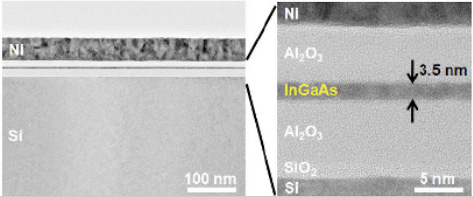
A team led by University of Tokyo wafer-bonded InGaAs alternative channel material to silicon to form dual-gate MOSFETs on an insulating substrate. (Source: IEDM 2010)
The limits of the single-gate bulk silicon CMOS transistor seem to be upon us, despite extensive use of strain and other clever extension tricks. For 22nm node devices, there is excessive variability due to channel doping variations (<100 dopants atoms per channel), gate leakage, and parasitic capacitances. Such issues have been known for years, and researchers have developed various known ways forward, including the use of a silicon-on-insulator (SOI), alternate materials for the channels such as germanium (Ge) and indium-gallium-arsenide (InGaAs, figure), as well as dual- and tri-gate transistors.
So far, SOI has been used by IBM and AMD for microprocessors and by all video game makers for the main brains in their boxes, but there is major additional cost for the substrate and so most commercial fabs do not run SOI wafers. Multiple gates have been pushed out again and again. Trigate transistors—a.k.a. “finFETs” and many variant names for their cross-sectional shapes—have long offered superior performance for minimal additional cost, but EDA models didn’t exist for such devices and so it was difficult to design them into commercial ICs. Now these technologies are under consideration for high-volume use in the next few years, as will be shown in presentations at IEDM 2010.
Fully-depleted SOI (FDSOI) is claimed by CEA/Leti/Minatec [Session 3.2] to be easier to integrate than non-planar devices like finFETs. This paper will address electrostatic integrity, drivability, within wafer variability, and scalability with silicon data down to 18nm gate lengths. Solutions to the challenge of multiple VT transistors and non-logic devices (ESD, I/Os) will also be reported.
Dual-gate FDSOI work-function control to tune multiple VT levels will be shown by CEA/Leti/Minatec along with ST, Soitec, and Aixtron [Session 3.4]. By work-function engineering of TiN/TaAlN metal gates, short channel performance of 500µA/?m ION and 245?A/?m IEFF at 2nA/?m IOFF and VDD=0.9V will be reported on pMOS with a TaAlN gate. The combination of two metal gates with either n- or p-doped ground planes below the Ultra-Thin Buried Oxide (UTBOX) can offer 4 different VT from 0.32V to 0.6V for both nMOS and pMOS. Most of the same researchers will later show [Session 11.2] high-performance planar multi-gates devices with a Si-conduction channel of 4nm, allowing drive current up to 1350µA/µm @Ioff=0.4nA/µm. Vitally, this paper will also show how to self-align the two planar gates, based on, “the direct exposure of a HSQ layer through a 5nm Si-channel.” This opens the way to an easy planar multi-gate process for ultimate CMOS, fully co-integrable with conventional devices.

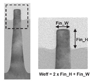
SEM cross-section of finFET from TSMC's complete high-performance 22/20nm CMOS logic technology, featuring SiGe stressors, metal gates, and high-k dielectrics. The FinFETs were used to build a dense 0.1µm2 SRAM memory cell. (Source: IEDM 2010)
FinFET architectures will be shown twice by TSMC to be ready for 22nm node fabrication [Sessions 27.1, 34.1]. The company will present on a high performance 22nm bulk finFET (figure) that achieve “best-in-class” Ion of 1200(N)/1100(P) uA/um for Ioff=100nA/µm at 1V. Dual-Epitaxy and multi-stressors are essential to boost the performance of dual workfunction HKMG transistors. The company’s abstract claims that finFETs, “the transistor architecture of choice for high performance CPU applications, can also be extended for general purpose SoC applications by proper device optimization.” For low-operating power applications, significant Ion improvement and Ioff reduction are claimed through EOT scaling and mobility improvement. N-finFET and P-finFET achieve ION of 1325 µA/µm and 1000 µA/um at 1 nA/um leakage current under VDD of 1 V, respectively.
Due to ever increasing complexity and cost, the real details of next-generation fab processes are generally kept secret. Even when discussed, there is always the possibility that the information presented is a dead-end with hidden problems. Novel technology may work, but may come with unacceptable side-effects like cost increases and yield losses. Managing the complexity of process technology interactions, and knowing which processes to deploy at the right time establishes the typically slow pace of evolution.
So finFETs remain attractive but are probably more challenging to integrate compared to alternate channel materials, and unless TSMC has made a big hidden investment in EDA modeling they probably cannot be designed into mainstream 22nm node ICs. Planar dual-gates are probably the best bet for the next major transistor architecture, so long as a self-aligned approach can be made to yield well. However, even dual-gates may be pushed out past 22nm, since alternate channel materials will likely be used at 22nm and should provide sufficient performance. If so, then the 16nm node would be the first use of dual-gates with or without FDSOI, and finFETs would be pushed out indefinitely.
The best way to understand this complexity is to attend IEDM and talk to the manufacturing folks who have to make it happen one way or the other. If you cannot attend in person, the conference organizers have created a page on Facebook, and they will be posting tweets to Twitter including paper titles and links to the technical program sessions. IEDM also includes the latest and greatest presentations on power electronics, memory cells such as Flash and upcoming ReRAM, RF and ultrafast ICs, CMOS image sensors (CIS), and devices results using everybody’s current favorite sticky-tape-your-way-to-a-Nobel-Prize-material graphene. A plenary talk entitled “Energy Efficiency Enabled by Power Electronics” will be given on the first day by Arunjai Mittal of Infineon Technologies. Stay tuned. –E.K.
Tags: 22nm, analog, CEA/Leti, CMOS, dual-gate, FDSOI, finFET, graphene, IC, IEDM, Infineon, Intel, memory, MEMS, Mittal, ReRAM, RF, SOI, transistor, tri-gate, TSMC
