Friday, November 26th, 2010
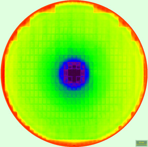
On November 16 of this year, the IEEE San Francisco Bay Area Nanotechnology Council held a symposium on nanomanufacturing that included presentations by TSMC and GlobalFoundries (GloFo) on gate-last (GL) versus gate-first (GF) high-k metal-gate (HKMG) integration. Control of non-visible defects (NVD) in manufacturing is vital, particularly for GF flows, and such control is provided by patterned wafer work-function metrology from Qcept Technologies (figure), though this newer metrology capability was not discussed during the IEEE event.
One of the biggest technology issues in commercial IC fabs today is how to integrate HKMG CMOS transistors at the smallest geometries. As previously covered by BetaSights, Intel and TSMC have chosen GL integration for the 3Xnm node, while GF has been chosen by IBM and GloFo and the rest of the world (except for UMC using both GF and GL).
The benefits of the GL (a.k.a. replacement metal gate or RMG) flow were presented by Di Ma, vice president of field technical support for TSMC North America. TSMC’s variant of the 32/28nm node uses HKMG for high-performance CMOS, while the foundry still provides traditional SiON/poly-gate CMOS for low-power chips. Restricted design rules (RDR) are definitely needed at this node.
It is universally acknowledged that the GF flow is derived from traditional SiON/poly-gate flows, while GL requires integration in new directions. “After thorough evaluation, TSMC has decided to take on the gate-last integration challenges,” explained Ma.
According to Ma, there are 5 basic advantages of GL over GF that justify the integration investment:
-
Faster ICs (mostly on the PMOS side),
-
Lower power (lower Vt allows lower Vcc),
-
Higher yield (reduced NVD issues),
-
Reliability (no high-temperatures post-gate),
-
Forward compatibility (more MG options for shrinks).
“I’m an old-timer,” said Ma, as he explained the history of commercial MOSFETs starting with NMOS poly up to today’s CMOS HKMG. Regarding the HKMG flow choice for the 32/28nm node, Ma asserted that the industry would, “probably have to use gate-last by 22 or 20 nm anyway.” Forward compatibility is helped by greater flexibility in being able to tune the work-function of metals after all the highest temperature processing of oxides and nitrides.
Ma said that 28nm SiON/poly has passed full qualification at TSMC, and that 28nm HKMG is now “on track.” The company claims to have already engaged with 40 customers for 28nm node ICs, with first production tape-outs in this quarter, and 50 tape-outs expected in 2011. However, Ma did not specify the split between SiON/poly and HKMG for all of these ICs.

ChemetriQ charge map of a 45nm node GlobalFoundries CMP wafer from a malfunctioning cleaning tool. The dark blue region at the center was charged to -4.5V, which was sufficient to cause yield loss of all the dice in that region. Prior to this charge map being generated, GlobalFoundries had taken this tool offline because of the yield issue with no correlating defectivity reported by optical inspection tools used at the fab. (Source: Qcept Technologies)
“If there are defects in electrical parameters they are difficult to find until the very end of processing,” reminds Ma, explaining why TSMC prefers to take on the known visible defects associated with GL. Proven technology to defect NVD may not have been available when TSMC had to choose it’s integration scheme, but such capability has existed since this summer when Qcept released the ChemetriQ5000 tool to provide work-function measurement on patterned wafers (figure).
Nick Kepler, GlobalFoundries vice president of corporate program management, summarized the good reasons to choose GF HKMG for the next node:
-
Backwards compatibility (to SiON/poly), and
-
Design flexibility (fewer restrictions needed).
“First of all, when we introduce new materials we look at how to make the change as simple as possible to minimize risk,”explained Kepler. “The gate-first implementation is the most similar to polysilicon. The second is we wanted to put as few constraints as possible on the design teams. With gate-first we can allow for things like bi-directional poly, poly jogs, and large caps.” Kepler claimed that such design flexibility allows GloFo to get to 20-25% smaller overall die size compared to GL.
However, when you compare GloFo’s 32nm relaxed designs with TSMC’s more aggressive shrink to 28nm restricted designs, the area results are probably about the same. Kepler also reminded the audience that GF flows allow for significant Vt tuning through the use of monolayer oxides, and that GloFo offers multiple Vt levels to it’s customers.
If GF and GL flows provide similar die sizes with similar overall circuit performance, the main difference may be in the yield numbers, and fab yield is controlled by metrology and inspection tools. Last summer, following successful beta-site evaluations at an unnamed fab, Qcept announced the first sale of a ChemetriQ5000 tool capable of patterned wafer NVD inspection with 0nm edge-exclusion. In a meeting with BetaSights in July of this year, Qcept vice president of marketing Ralph Spicer explained that this new tool uses a ~30 micron diameter sample area with a continuously rotating stage to provide ~15 wph throughput. –E.K.
Tags: 32nm, CMOS, fab, GF, GL, HKMG, IC, IEEE, metal, metrology, NVD, PMOS, poly, RMG, SiON, yield

