Monday, November 29th, 2010
Rarely does the IC fab world see a really new tool. The shear complexity of multi-million dollar tools automated for high-volume manufacturing (HVM) means that changes are usually gradual and evolutionary. Today, Applied Materials officially announces the new “Centris” higher-throughput platform for etch, targeting formation of transistor as well as the sacrificial structures needed in sidewall-spacer double-patterning for lithography.
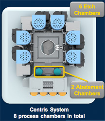
From a first glance (figure), Centris for etch is modeled on the company’s Producer platform for deposition, with a dual-blade robot handling wafers to and from parallel chambers. The new platform deals wafers to AdvantEdge MESA chambers that have previously run on the Century platform (>1500 AdvantEdge chambers shipped since 2001, and >200 MESA chambers in the first 9 months of release). When fully loaded with 6 etch chambers, the tool is claimed to be able to process 180 wafers-per-hour.
Each of the chambers in a set of two has separate high-vacuum pumps and gas delivery sub-systems, allowing process recipes previously developed for MESA chambers to be run on the new platform. However, each set of two chambers shares heat-exchangers, roughing pumps, facilities gases, and cooling water to reduce costs and fab floor space. Compared to Centura MESA etch processes, the company targets a 30% reduction in the cost-of-ownership (CoO), with ~1/3 of that (or ~10%) derived from energy savings alone.
Significant new sub-systems in the Centris platform include the following:
-
Bromine-abatement integrated into the load-lock,
-
Four FOUP interface, and an
-
Optimized gas panel for chamber matching.
The new gas distribution sub-system includes all lines to chambers of equal length (for chamber matching), and the ability to share a single input manifolded to six. However, the degree of control needed for 32nm node etching is such that the best designed sub-systems will still experience parameter drifts during manufacturing. As such, periodic sub-system calibration to some reference standard is now part of standard fab routines, and this new tool automates the calibration process. A mass-flow standard (with rate of rise) and a manometer are integrated into the hardware platform, and software automatically trigger calibrations during chamber during down-times. In an exclusive discussion with BetaSights, Thorsten Lill, Applied Materials’ vice president of the Etch Business Group, stated that the chamber base pressure repeatability using auto-calibration was within the range of 0.1 mTorr.
“Conductor etch” is one of the fastest growing IC fab OEM segments. In part due to the challenges of forming new transistor and isolation structures (figure), but also due to double-patterning (DP) and hard-mask etch falling into this categorization. While some manner of DP will be used for many critical layers at the 32/28nm node, there are still many variations on the theme. Even within a general process flow like sidewall-spacer DP, there will be sub-variations. Even within sub-variations, the process window is so slight that there probably will be no “universal patterning” flow that works for all layers. “In reality, you see slight tweaks for dense-iso requirements,” explained Lill. “For example, you could have a scheme where two spacers are too close.” Each fab chooses the detailed DP flow based on differences in the material layers to be patterned, as well as on the legacy tools running in the line.

SEM cross-section of NAND STI structures etched using double-patterning and the MESA Pulsync technology to minimize micro-loading (source: Applied Materials)
For almost any double-patterning approach, etch now provides the most essential control of the patterning. As such, the post-process critical dimension (CD) variation must be minimized though both control and matching of chambers. A 4000 wafer run of 40nm test-element groups (TEG) through 4 chambers on a Centris reportedly demonstrated 0.8 nm range.
In other etch news, the company has also released a new “ultra” high-density plasma (HDP) Silvia chamber for the Centura platform, primarily targeting through-silicon via (TSV) formation. The company claims a 40% higher etch rate with the new source. —E.K.
Tags: 32nm, Applied Materials, CD, Centris, Centura, control, CoO, DP, etch, gas, HDP, HVM, IC, litho, MFC, OEM, Silvia, TSV, uniformity

