Tuesday, December 14th, 2010
TSV are finally finding problems to solve. As previously covered by BetaSights, through-silicon vias (TSV) for 3D circuit stacking will first be used in silicon-interposers (formerly known as silicon-substrate multi-chip modules, “Si-MCM”), as indicated by Xilinx’s announcement of high-end FPGAs requiring the nascent technology. Now IBM has teamed with Semtech to announce plans for a new silicon-interposer ADC/DSP product family that has applications in fiber optic telecommunications, high performance RF sampling and filtering, test equipment and instrumentation, and sub-array processing for phased array radar systems.
Semtech (the analog and mixed-signal IC company) is partnering with IBM to develop an end-to-end module solution using IBM’s 3D interposer technology to interconnect ADC functions in IBM custom logic SOI-based Cu-45HP technology with interleaver ICs in IBM’s 8HP BiCMOS SiGe technology. These two different technologies are connected through a single wiring layer on an interposer, which supports a bandwidth of greater than 1.3 Tbps in this design. Semtech will have first ADC/DSP prototype modules available in 2011 and are working with partners to extend these product offerings utilizing these technology elements.
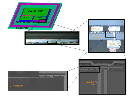
IBM’s 3D technology combines cost effective 90nm BEOL wiring levels with copper (Cu) TSV (figure). The fact that IBM is now on-the-record as using Cu TSV for production is surprising and may be a classic example of technology mis-direction, since most of the previously published papers on TSV technology development by the corporation used tungsten (W) metal instead of Cu. IEDM this month included a presentation by IBM and National Chiao Tung University titled, “Reliability and structural design of a wafer-level 3D integration scheme with W TSVs based on Cu-oxide hybrid wafer bonding.” Of course, the W TSV are supposedly intended to go through dice with active circuitry, while the Cu TSV are so far only announced for interposers.
Regardless of the via metal, integrated passive components provide superior performance in system-in-packages (SiP) using silicon interposers. IBM has developed the ability to provide ultra high capacitance density by integrating deep-trench (DT) capacitors at the top surface of the interposer. As frequency increases, the use of integrated decoupling capacitors is more attractive to counteract power supply noise effects that typically may be second order issues for slower applications.
“3D technology provides a path to integrate CMOS and SiGe technology at very high bandwidth and with low power to provide a seamless high-performance module solution,” said Dan Berger, IBM Manager of 3D Technology Development at its Semiconductor Research and Development Center (SRDC). IBM’s semiconductor, wafer finishing and assembly facilities offer a one-stop module solution for Semtech and its product partners. We also see significant benefits using 3D technology for other applications to address issues such as I/O power, power supply, interconnection bandwidth between components, modularity for re-use of IP or mixing technology nodes effectively, and form factor improvements that can be obtained by integrating components together in a smart cost effective manner.”
IEDM 2010 TSV updates
Since the recently concluded IEDM in San Francisco placed more emphasis upon “More-than-Moore” technologies, there were two sessions covering 3D including TSV. Session 2 was titled, “Process Technology – Advanced 3D Integration,” while a special invited session (#17) was on the, “Confluence of Technology and Design – Challenges for Non-Conventional Devices and 3D LSIs.”

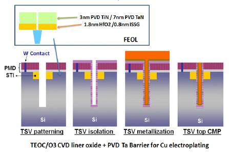
Schematic of the gate stack under test and the main technology options implemented in IMEC's 300mm High-k/ Metal Gate First CMOS 3DIC via-middle baseline. CMOS is done until contact level then the Cu-TSV module is inserted, followed by BEOL. (source: IEDM2010, Session2.1)
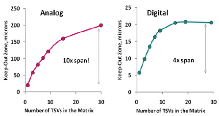
IMEC researchers used a via-middle Cu TSV process flow to examine the Keep Out Zone (KOZ) requirements for active circuitry (figure). TSV induced stress changes with temperature as the tensile copper expands faster than silicon when heated. The TSV KOZ is expected to disappear at the stress-free Cu temperature of 145°C. The researchers experimentally demonstrated a significant influence of TSVs on adjacent transistors, with up to 30% Idsat shift due to TSV stress. The KOZ for a large matrix of TSVs is over 200 microns for analog circuits and 20 microns for digital circuits (figure). The complex interactions of stress components makes it difficult to use simple design rules without sacrificing large layout areas. The issue of induced stress and uncertainty in active circuitry KOZ rules is only one of the reasons that TSV are today only designed into passive interposers.

Keep out zone for analog devices with 0.5% delta-Ion sensitivity threshold and for digital devices with 5% delta-Ion sensitivity threshold as a function of the number of TSVs in the matrix. (source: IEDM2010, Session2.1)
The first presentation in the reliability session (#35) covered research led by CEA-Leti on, “Investigation on TSV impact on 65nm CMOS devices and circuits.” Using 4 micron diameter Cu TSV, they ran electrical tests on isolated MOSFET transistors as well as on ring-oscillators. Noise spikes of 7uA/um were reportedly observed in the static source current of nMOSFETs at 5 microns distance; this corresponds to ~1% fo the saturation current. However, no mobility degration was observed in the ring oscillators. –E.K.
Tags: 65nm, 90nm, ADC/DSP, CEA-Leti, Cu, FPGA, IBM, IC, interposer, MLM, Semtech, Si, TSMC, TSV, W

