Wednesday, February 18th, 2009
For thick plating applications like copper pillar bump processing in semiconductor advanced packaging, Shin-Etsu MicroSi has introduced a positive tone, ultra-thick photoresist, SIPR-7126. The 7100 chemically amplified (CA) series has been in production for several years, and the SIPR-7126 has been optimized to reduce processing steps and improve removability in layers up to 100 µm thick. The new material with be shown at the SPIE conference and exhibition, Feb. 24-25, at the San Jose Convention Center in San Jose, California.
This i-line photoresist was developed to plate high aspect-ratio features, like those used in copper pillar processing, and GaAs and MEMS devices. These special applications need an ultra thick layer of photoresist to help cover topography on the integrated circuit and to plate very high aspect ratio features. The material reportedly provides highly vertical sidewall profiles, so that Cu plating can easily form proper pillar cross-sections. The plating chemistries are complex and varied so the resist must also be chemically robust.

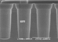
60x180 µm TSV etch; profile angle 70° for top 30 µm, then 88.8° down to 180 µm (source: AlcatelMMS, transferred 2008 to Tegal)
The resist is also applicable to semiconductor etch applications, like MEMS and through-silicon vias (TSV), where process engineers must etch tens to hundreds of microns of silicon to build the device circuitry (see figure). The new photoresist features include:
* excellent flexibility with different plating chemistries, and
* no post exposure bake needed, which allows for
* easy removal and rework.
Shin-Etsu MicroSi, the wholly owned subsidiary of Shin-Etsu Chemical Co., headquartered in Phoenix, Arizona, created this flexible i-line photoresist so that it can be developed by standard TMAH solutions. This new photoresist—which can be coated up to 100µm thick in a single pass—is available for sampling and evaluation now by contacting Shin-Etsu MicroSi. –E.K.
