Tuesday, September 7th, 2010
On August 31st, HP announced that it’s memristors and circuit-smarts will combine with Hynix’s manufacturing prowess to bring resistive RAM (ReRAM) chips to commercial markets in three years. HP Labs’ leader Stan Williams says that ReRAMs based on his team’s titania resistor should be able to switch 10x faster than 22nm node NAND Flash, and do so with 10x lower power consumption using unique circuit architectures and error-correction codes. HP’s corporate communications team worked to ensure that both mainstream and technology media reporters were briefed on this news, but most reports merely restate the press release. Refreshingly, Mark LePedus at EETimes provides the best overview of the non-volatile memory (NVM) marketplace, while ace technology reporter David Lammers freelances for the IEEE about the motivation for such a technology.

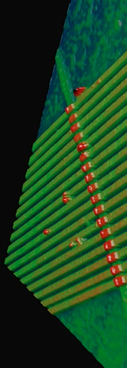
AFM image of 17 memristors formed at the titania cross points of thin nano-bars of platinum. (Source: R. Stanley Williams, HP Senior Fellow and Director, Information and Quantum Systems Lab, HP Labs)
However, only at BetaSights can you learn why HP leads with the materials engineering of memristors, how Stan Williams’ lab at HP has developed cross-bar architectures (figure) for ReRAMs over the last decade, and what issues remain to be solved before high-volume manufacturing (HVM) can commence at Hynix. This editor has toured the lab, and seen Williams present memristor details at Materials Research Society meetings, and the best source for technology information about memristors is still the April 22nd BetaSights post, “Memristor manufacturing for memory, logic, and AI.” Go back and read it again, before continuing with this analysis of the deal with Hynix.
ReRAM work started at HP Labs ~2000, but it was only 2006 that the specific titania-based memristor device was found, and only in the last year or so that the non-electroforming PVD fabrication method was developed. As reported after the MRS spring meeting, many companies and universities are exploring memristor devices using other oxides besides titania that can be sandwiched between electrodes in cross-bar structures, but all other teams are still stuck with the need to use an expensive and unreliable electroforming step. Only HP has made the critical breakthroughs in both theory and practice that allow memristors to be formed inexpensively and reliably, and with IP protection for Ti4O7 PVD integration the company seemingly owns the only known way forward using titania.
Why do HP and Hynix think that it will take three years to move this from lab to fab? Well, the issues are not just integration and yield, but some of the most critical basic unit-processes may have to be completely re-done on Hynix’s R&D line. Deposition will almost certainly remain PVD for both electrodes and storage layers, since everything is planar and the process relies upon the stoichiometry tuning possible with PVD targets. However, the patterning to date has used a manual home-brew nano-imprint lithography (NIL) tool, and either a commercial NIL technology or a sidewall-spacer double-patterning (SSDP) approach will be needed for 300mm wafers. Also, the lab uses the ancient and messy technique of “lift-off” in a wet bath (note many defects in the figure), and some manner of dry etch will almost certainly be required for HVM yield. The etch of the platinum electrodes will be tricky, but there are known approaches using either SF6/Ar or O2/Ar plasmas.
The fast reversibility of 22nm titania memristors—due to the diffusion of oxygen-vacancies across just 1.2nm—is key to the many potential memory applications that could be served by ReRAMs. Many oxides and organics can be found that switch once for limited PROM applications, or switch slowly for niche NVM applications. Old technologies like MRAM and FRAM—both read as resistance changes—cannot function at 22nm due to the need to write cells with fields across larger plates. Phase-change RAM (PRAM, a.k.a. PCM, OUM, etc.) can be fast and tiny, but relatively more costly due to the need to integrate heaters and drive transistors.
We’ve heard about “ubiquitous” memory chips on the horizon many times before, and none have yet arrived. Only NAND Flash has even moved toward ubiquity by replacing HDD for a few niche applications, but while creating it’s own huge space in the mainstream it has failed to replace any established memory chip technologies. The clock is now ticking. If HP and Hynix are successful, the 22nm node memory market in 2013 will include ReRAM wafers made with costs and yields near Flash. If so, then the far superior densities and functionalities of memristors-based ReRAMs would result in a new leader setting the pace for Moore’s Law, and foundries (and maybe other memory IDMs) would have to see what the going price is for licensees. Terms of the JDA, such as how hypothetical licenses might be issued, have not been disclosed.
Besides ReRAMs, HP researchers have already shown that memristors can function as both 3D interconnect layers and latches for complex digital logic circuits. Researchers in Iran have discovered that two memristors in series precisely mimic the analog dynamics of human neurons, further justifying hope that learning circuits could finally lead to practical artificial intelligence (AI). Memristors now seem significantly closer to providing real fun and profit.–E.K.
Tags: 16nm, 22nm, AI, DRAM, etch, Flash, HDD, IC, litho, logic, memory, memristor, NAND, PVD, R&D, ReRAM, SSDP
