Wednesday, January 27th, 2010

… and after years of tribulation with most people gone to other lands, a great fear was upon the land of Publishing for all business models were lost along with all hope. The web had washed so much away, and the multitudes prayed that the one true Jobs would intervene and with compassion bestow upon the world a great new Device and Transaction Services Thereof. And having agreed to foresake all other OSs, the prayers of the multitudes were answered today when Jobs revealed the iPad. And they saw that it was good.

This is the 100th BetaBlog post, and today is the day that Apple released the iPad. Consequently (unlike most posts about high-tech manufacturing; try clicking in the Tags-cloud, Categories, or Archives), this is about the business of publishing and the dynamics thereof. Ancient Greek theatrical stagings often involved a person playing the role of a god (Lat. “Deus”), who would appear from (Lat. “ex”) the top of the stage being lowered by a machine (Lat. “machina”) to resolve difficult plot twists; consequently, “deus ex machina” has come to mean something like devine intervention. The commercial publishing industry—long suffering from a broken business model with no hope for the future—has been praying for just such a “Jobs ex machina” intervention.

Ever since Stewart Brand said something that included the phrase “information wants to be free” in 1984, without particularly contemplating the ramifications, most people have thought that for some reason information should be exchanged without a transfer cost. The architects/designers who developed internet software over the last 25 years did so with the idea that information will flow without transfer costs, and that any money involved would be made by ISPs and access device makers.

Starting with digital audio recordings of popular songs, Apple created the iTunes internet store. In so doing, iTunes established a vital new business model and distribution method during a period when nothing else worked. At this point it is not absurd to say that Apple led by Jobs saved the music industry.

The most recent attempt by the publishing industry—specifically Time, Condé Nast, Meredith, the News Corporation and Hearst—to save itself was the recent creation of the Next Issue Media consortium that plans to run its own online store selling digital issues and collecting consumer information. “It’s fundamental to the business model of publishers. We’ve always enjoyed an opportunity to know exactly where our consumers are, and be able to market other products to them,” said John Squires, the interim managing director of the consortium. “It’s a very key issue for the founding members of this business.” The consortium includes only some of the world’s major publishers, and they have not yet disclosed details of their “open” standards, so this direction is still uncertain.

Meanwhile, Apple’s new iPad will use the EPUB electronic publication format, which is also supported by Adobe’s Digital Editions software. With all EPUB files to be distributed through an Apple website, just as people are willing to pay a few dollars for audio and video files, people may soon get used to paying modest amounts for electronic books, magazines, newsletters and dailies (figure). Publishers will lose control of their audience to Apple, but Apple will provide a paying and growing audience.

Though we knew that a subscription business model was a risk, BetaSights was originally founded one year ago to sell niche specialized newsletters. However, due to the conceptual momentum of the recent past, most people were not willing to pay for a newsletter and so we stopped its publication. This blog page remains as an example of our topical expertise and writing style, while we have spent more time on consulting projects for clients.

Now that the iPad and transaction services thereof have been revealed to the world, we all have a few months to get used to the possibility of a major change in our information world. Perhaps a day will come when everyone will see that information is valuable (not free), and that value varies with quality. After a while, we’ll probably all get used to subscribing to a few quality niche e-newletters. At that time, maybe the BetaSights Newsletter will re-exist as one of your favorities…—E.K.

Friday, January 22nd, 2010

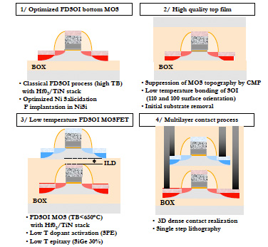
The IEEE’s International Electron Devices Meeting (IEDM) is still the place to see the latest micro- and nano-electronics research targeting commercial markets. On December 8, 2009, French researchers from Leti/Minatec showed “3D sequential CMOS integration” as <600°C processing of PFETs using a (110) orientation FDSOI layer that was transferred on top of NFETs made using traditional (100) orientation wafers.  A decrease by 4Å of the PFET Equivalent Oxide Thickness (EOT) is measured using the <600°C process. Electrostatic coupling between stacked FETs is demonstrated, enabling 22nm node SRAM stabilization through a 130mV dynamic shift of threshold voltage.

With complimentary metal-oxide semiconductor (CMOS) devices now shrunk down to 32nm scale in production, and 22nm in development, the industry has done almost all that can be done in 2D. Thus, the motivation to explore the 3rd dimension, and the interest in finFETs (3D transistor structures) and through-silicon vias (TSV for 3D stacks of circuits). TSV are used to connect together two or more silicon IC layers that were independently fabricated in parallel. This exciting new work from Leti connects together two silicon IC layer that are fabricated sequentially (figure).

Most of the fundamental unit process steps needed to do this work seem to have been known in prior art, but no one had combined everything together to create such a novel circuit structure. Previous work by Tracit (now part of Soitec) had shown the possibility of doing thin-film transfers of silicon from one wafer to another with structures beyond blanket layers. From first principles of materials engineering, dopants can provide grain-boundary “pinning” that slows grain growth during thermal exposure. Relatively rapid SiGe epitaxial growth at <600°C has been shown.

The bottom NFET layer of transistors use a 5mn HfO2 and TiN/Poly-Si(N+doped) gate stack. Raised source/drain (RSD) structures were formed by salicidation of Ni, then an innovative fluorine implant step stabilizes the NiSi such that it can withstand the thermal budget of the top PFET processing to come. The sheet resistance of the NiSi(F) blanket film is 12-14 Ohms-square as formed and after the thermal budget exposure of top layer processing. Deposition of the thin Inter Layer Dielectric (ILD) followed by CMP to eliminate topography, provides the surface for the 200°C molecular bonding of a SOI substrate as a perfect quality top active layer.

Top MOSFETs are then processed with an overall thermal budget limited to 600°C:
•    HfO2 anneal 515°C (5 min),
•    Poly deposition 515° (40 min),
•    Spacers deposition 480°C (time not specified), and
•    SPE dopant activation 600°C (2 min).

In addition to Solid Phase Epitaxy (SPE) for dopant activation, this flow uses SiGe epitaxy at 600°C to form RSD. For 30% Ge, 4nm/min growth rate has been obtained. To optimize the PMOS layer (above the NMOS), in situ B-doped SiGe RSD were also tested.

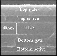
Functioning circuits have been created using this approach, including an equilibrated inverter with (110) PFETs on top of (100) NFETs, and a 3D SRAM with (100) load PFETs stacked on (100) drive and access NFETs. The unique 3D electrostatic coupling between layers was quantified depending on the targeted ILD thickness:  for 120nm thin ILD the top transistors can be considered as FDSOI with thick BOX, while for 60nm ultra-thin ILD the result is a Double Gate like device (figure). In the latter case, a 130mV threshold-voltage shift is observed when the top NFET lies above a bottom transistor, demonstrating that the threshold voltage of top FETs can be dynamically tuned by biasing bottom FETs so as to stabilize SRAM cells.

This work shows that there are many ways to go “3D” with ICs. By stacking layers closely together, we achieve a new degree of freedom in circuitry:  dual-gate devices when needed, or double the number of transistors per unit area of silicon. Compared to parallel integration using TSV, sequential integration provides unbeatable results in one basis parameter: overlay error. Layer-to-layer alignment using TSV generally targets ~500nm, while this manner of stacking allows for ~10nm precision! –E.K.

Tuesday, December 1st, 2009

Based on proven hardware sub-systems from previous models, Applied Materials has released a new chemical-mechanical planarization (CMP) tool that processes two 300mm diameter wafers simultaneously on each of two plattens. Initially targeting copper interconnect formation for memory ICs, the Reflexion GT tool has passed betasite tests at multiple customers, and reportedly provides 60% higher throughput than competing tools while requiring up to 30% less slurry use.

“Today’s copper-based logic and memory devices have more copper interconnect layers, requiring faster CMP processing and more efficient use of consumables,” said Lakshmanan Karuppiah, general manager of Applied’s CMP business unit. “In addition to its high speed throughput, this new architecture allows customers to realize substantial savings in the cost of consumables, which typically comprises 70% of the total cost per wafer.”

However, we live in a world of trade-offs. In this case, to acheive the lower cost-per-wafer, the tool has only two plattens (see figure) instead of the three found in the company’s previous tools. When establishing a new process of record (POR) for a new line, such as DRAM fabs that are just now transitioning from aluminum to copper interconnects at the 4Xnm generation, it can be cost-effective to start from the beginning with different tools and consumables. For lines already established with three-step recipes that need to add capacity, or for new lines that cannot afford to do more than tweak an old three-step POR, standard three-platten CMP tools will still be required. So these new two-platten tools are really made for new lines.

After planarization is complete, a parallel-path, clean module using proven Marangoni vapor drying delivers highly-effective, water mark-free wafer cleaning. With all of the doubling, modeling a 30k wafer-starts-per-month (wspm) logic fab or a 120k wspm memory fab, Applied Materials claims that seven of these new tools would be needed compared to eleven of “the competition” (presumably Ebara).

How do the consumables costs get reduced? Since the pad is 42” instead of 30”, double the size for double the wafers results in equal pad wear over time, and the larger pad will cost less than double so the pad cost/wafer will improve. Slurry use/wafer is reduced in two ways: lower pad rotation rate reduces the centrifigal force that sluffs it off the edge, and the two wafers share some of the used slurry between them. There is dedicated slurry dispense and pad-conditioning for each head, so that both wafers see the same fresh slurry and pad condition.

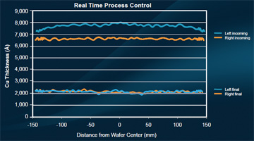
An insitu eddy-current sensor was used on the prior Reflexion LK tool for within-wafer process control; the sensor’s signal feeds to the Titan Contour wafer holder (“head”) where the back-pressure on the wafer is automatically adjusted. The result is significant improvement in uniformity for each wafer, and the key to the ability to independently control the process uniformity of two wafers on the same platten in the GT tool. The company shows the ability to even “heal” thickness variations between the two wafers (see figure). In today’s fab world of almost vanishingly small process windows, the ability of a tool to reduce the variability of an incoming device structure is truly wonderful. Optical end-point sensors complete the bulk metal and dielectric/barrier process control.

The Reflexion GT system is available now for copper interconnect planarization and has claimed demonstrated extendibility to tungsten applications. This innovative system adds to the company’s decade of leadership in CMP technology, with more than 2,700 systems at customer sites worldwide. For more information, including an animation showing the wafer handling, visit the company’s website. –E.K.

Friday, November 13th, 2009

Intermolecular, the company that brought combinatorial chemistry to semiconductor manufacturing R&D, has expanded its focus to look at ways to improve basic manufacturing processes for photovoltaic (PV) fabs. “I think that the PV devices of 10 years from now will look significantly different from those of today,” said Intermolecular vice president and general manager of solar and energy technologies Craig Hunter in an exclusive interview with BetaSights. Perhaps independently, Caltech and Dow will be working on low-cost thin-film PV in a four-year program that will certainly use some manner of combinatorial exploration.

The commercial PV fab industry has seen tremendous efficiency improvements over the years: crystalline silicon (c-Si) cells now provide 20-22%, multi-crystalline silicon (mc-Si) cells cost less and provide 15-17%, while thin-film PV panels are now under production at 7-11% using amorphous silicon (a-Si), mc-Si, CdTe, and CIGS absorbers. There is still room for improvement in efficiency for most PV technologies, and fab cost reduction remains essential since market demand is highly price-elastic.

Starting with high-productivity combinatorial (HPC) technology developed by Symyx Technologies—including over 650 granted and pending patents—Intermolecular has developed its own portfolio of over 90 granted or pending worldwide patents that deal with process R&D. Intermolecular has assessed the current status of R&D in PV companies as lacking the ability to thoroughly and cost-effectively explore process spaces.

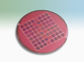
To be sure, it is a long way for a new technology to go from a champion PV cell in the lab to $/kWh panels delivered into the field in volume. Combinatorial parallelism allowing for 64 experiments on a single wafer (see figure) certainly accelerates experiments, which leads to faster time-to-knowledge. The company can form 18 different cells on a single mc-Si wafer. Intermolecular’s combination of hardware parallelism integrated with an information database makes it possible to explore both faster and a greater area within the process space.

Existing fab lines need to be able to explore the edges of process spaces, and to look at complex multi-dimensional interactions. The goal is both cost reduction and line stability. For example, through exploring process interactions we might discover that the thickness of a vacuum film deposition was particularly sensitive to temperature variations across the substrate, but by using a different optimal vacuum level we can find the thickness is far less temperature dependent. Such exploration is possible with custom R&D tooling and expertise, but practically impossible on a production line.

While potassium-hydroxide plus isopropyl-alcohol (KOH + IPA) is the standard solution for Si surface texturing, Intermolecular claims to be developing a new solution that will provide at least equivalent texture with a wider processing window at significantly shorter process time. Some other PV fab technologies being explored by the company are as follows:

  • Crystalline Si: wafer texturing, materials for litho-less patterning of cells, enhanced front and backside passivation,
  • Thin-film Si: TCO composition and morphology, absorber structure for higher efficiency and improved stability,
  • CdTe: back contact and TCO for improved cost and efficiency, and
  • CIGS: higher efficiency, wider absorber deposition windows (wet, PVD), Cd-free buffer layer, improved durability TCOs.

Tony Chiang, Intermolecular CTO (founder of ALD technology company Angstrom, prior to its 2004 acquisition by Novellus), explains that PVD technology developed for IC phase-change memory (PCM) can apply to searching for an improved PV absorber. “A lot of the thin-films are similar to phase-change-memory materials,” said Chiang. “If you think about it, there are three base elements and a dopant material. It’s very analogous, and PVD is the way to address it.” Chiang proudly shows off custom built tools in the company lab with CVD, PVD, and PECVD chambers all connected to the same robotic vacuum handler, so that a single tool can also form backside contact and TCO.

For compound thin-film PV, there is a lot of potential to improve the performance of the fundamental absorber material. The two leaders today—CdTe and CIGS—rely upon relatively expensive rare-earth materials. While in principle there should be a lot of untapped potential to be found in complex combinations of common elements in the earth’s crust, such as iron (Fe), magnesium (Mg), and titanium (Ti).

Indeed, Caltech professor Nate Lewis (see figure) has been directing his researchers to experiment only with such common elements for many years now. Now his researchers will be working with Dow Chemical in a four year JDP to investigate the use of earth abundant elements to create new direct band gap PVs. “Use of earth-abundant materials can provide new technology options and could open new areas of design space,” notes Lewis. “This project will develop the science and technology base for thin-film solar-energy conversion using these widely available materials.”

Dow recently announced its first building integrated photovoltaic (BIPV) product, the POWERHOUSE Solar Shingle which uses a CIGS thin-film to provide low cost, easy installation, and a dramatically appealing aesthetic. Over a year ago, Dow announced that Global Solar would supply the CIGS technology for the first generation of shingles. –E.K.

Thursday, October 22nd, 2009

If EUV lithography is to succeed, infrastructure gaps will need to be addressed forthwith. The lack of inspection tools for EUV masks and substrates constitutes one such gap, now recognized as a priority by SEMATECH. At the OSA/APS Frontiers in Optics (FiO) meeting held in San Jose, October 11-15, Carmen Menoni of Colorado State University and an international team of co-authors showed how one key actinic mask inspection task might be accomplished.

The enabler for actinic inspection, according to Dr. Menoni, is a high-brightness EUV radiation source that is more convenient than the ones developed for lithography. The source presented at the FiO meeting was a table-top EUV laser at 13.2nm that uses a highly ionized (Ni-like) cadmium plasma to produce a beam with 2 microW of average power. That wavelength is close enough to the 13.5nm peak reflectivity of the multilayer stack of an EUV mask substrate to facilitate at-wavelength inspection.

The laser light goes into a simple EUV microscope where a Fresnel zone plate acts as a condenser lens to illuminate a test mask in just the way it would be in an EUVL scanner. The light reflected at a 6 degree angle is then projected and magnified by an off-axis zone plate objective with 0.06225 numerical aperture (NA) onto a CCD detector array.

With such a low NA, the zone plate resolution might not seem useful for defect inspection, but the objective has ¼ the numerical aperture expected for the first generation EUV exposure tools, which will have 4x demagnification. Thus, the image at the CCD is a magnified version of what would be exposing a wafer. Any anomalies in that image would correspond to printable mask defects. The optics train of the simple laser microscope is just what would be needed for a prototype EUV AIMS tool, the gold standard for mask inspection.

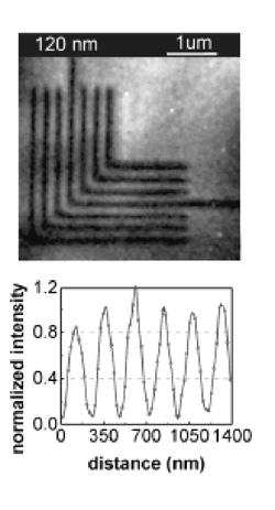
Initial results showed 55nm resolution in the mask plane, which would correspond to 14nm resolution at the wafer. Exposure time on 5m square nested elbow targets (see figure), however, was 20 sec and the initial images were degraded by laser speckle. Vibrating the condenser plate and averaging over 90 seconds produced higher quality images that might reveal subtle defects through die-to-database comparison.

The most remarkable feature of the system was that it all really did fit on a (rather large) table top and did not require a building sized synchrotron to function. Other talks at the meeting described improvements in extreme UV lasers. In particular, another Colorado State group described an all-diode-laser pumped soft X-ray laser at 18.9nm. If the efficient diode-pumped laser technology can be used with Ni-like Cd, much higher average power can be expected, leading to faster AIMS defect review. – M.D.L.

Friday, October 9th, 2009

Founded in 1984 with Flemish government support, IMEC has reached 25 years. To celebrate the organization’s accomplishments, BetaSights joined other industry media outlets attending a research review event in beautiful Leuven, Belgium. From 1999 to 2009 has been the “phase of international breakthrough” as described by current president Luc Van den hove. Working with OEMs such as ASML, in 1999 IMEC installed the first 248nm stepper—the PAS 5000/70—as one of the major sites for beta evaluations; 16 betas (or “pre-beta alpha”) have since been done for ASML. The IMEC Industrial Affiliation Program (IIAP) now works with most of the major OEMs in the world, as seen in the 300mm tools installed in the current fab.

These days, the consortium includes the “largest commitment of semiconductor companies into a partnership,” according to Van den hove. The Government of Flanders has provided steady funding over the years, but the vast majority of the 280M euro budget of FY2008 comes from industrial partners. Including loaned personnel from partners, the total size of IMEC staff is currently 4000.

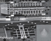
XSEM overview of IMEC’s standard and fishbone cantilever designs with suspended Pt trace and sharp tips (source: IMEC).

XSEM overview of IMEC’s standard and fishbone cantilever designs with suspended Pt trace and sharp tips (source: IMEC).

In 2000, Philips Corp. decided to consolidate CMOS R&D at IMEC, as the first “core partner.” With the motivation to develop a leading-edge 300mm pilot line, in 2001-2002 the Flemish government funded the start of 300mm fab construction in 2004. By 2005 it was ready, and by 2006 the full set of process tools were installed and other core-partners were attracted. Now a second 300mm line has been funded and is being constructed for official opening in June 2010. In addition, new fab space and personnel are being established to develop photovoltaics, biosensors, and MEMS (see figure).

Having built itself on core technology capability, IMEC now positions itself as provider of advanced system capabilities. The organization is involved in IP generation for configurable RF radio chips, human body sensors and networks, and photovoltaic manufacturing technology. “We are working at IMEC to develop functionalized nanoparticles…which could be used to treat tumor cells. One could also use them for localized drug delivery, which is much better than poisoning the whole body with something like chemotherapy,” said Van den hove.

Continuing CMOS scaling trends, “For 22nm, finFETs are being considered…resulting in better short-channel effects,” explained Van den hove. For extreme high-mobility channels, selective epitaxy of Ge and InGaAs are likely in the future. For memory cells, new TANOS materials (such as GdOx) and cross-bar technologies are also under development.

IMEC works with many universities, and also collaborates with competing international R&D centers such as Fraunhofer and CEA/Leti. SEMATECH’s EUV program dovetails with IMEC’s EUV since both used the “production alpha” tool from ASML, and both organizations have coordinated work on contamination and cleaning of masks and tools. “If there are opportunities, we will take advantages of them; we typically do things in a pragmatic way,” said Van den hove.

Rudy Cartuyvels, IMEC VP and GM Process Technology Unit, presented an overview of IMEC’s process integration capabilities for novel “More-than-Moore” IC applications. Through integrating new materials on the chip, in the chip, and/or below the chip, powerful new functionalities can be developed for volume manufacturing. However, the transition between an R&D site and a high-volume fab often results in delays and unexpected issues. Large and established integrated device manufacturers (IDMs) like Intel and IBM have sufficient resources to handle the transition from IC concept to product reality, but new and smaller companies need help.

With TSMC signed on as a partner (another old Philips tie-in), IMEC recently opened an R&D center in Taiwan. Now explicit connections have been established so that companies can do R&D with IMEC and then transfer production to TSMC for high-volume. “What we are offering with TSMC is a platform to enable the development of innovative product solutions using More-than-Moore technology options,” explained Cartuyvels. “IMEC and TSMC are very complementary; IMEC engages in the development of the technology and shows a functional prototype that is compatible with TSMC manufacturing base.” said Cartuyvels. IMEC has been working with TSMC for many years and there are many TSMC assignees in Leuven.

There are other R&D organizations in the world that offer outsourced process development capabilities, but their unit processes have not necessarily been established in harmony with a high-volume foundry. As the largest IC foundry in the world, TSMC has the deserved reputation for being able to deliver yielding chips built with the most leading-edge process capabilities.

“The whole process is customer driven. Today customers don’t know how there will be a path to high volume manufacturing,” said Cartuyvels. “The engagement of TSMC will depend on the market expectations for the process,” since there is a limitation on how many new technologies the foundry can handle. If the applications remains very niche and low volume then it could remain within the IMEC umbrella. The development phase for IMEC typically ranges from 1-2 years; during that time TSMC can invest in the technology manufacturing capability if they chose.

In addition to the work on system-level-integration and transfer to high-volume, IMEC continues to develop new core technologies for CMOS transistors, metal interconnects, photovoltaics, high-brightness LEDs, MEMS, biosensors, and 3D packages. BetaSights will be covering these developments in future posts. –E.K.

Sunday, October 4th, 2009

KLA-Tencor recently announced its long awaited 193nm reticle defect inspection tool, the Teron 600. Wafer scanners adopted 193nm exposure wavelength years ago in order to shrink circuit features below the resolution limit set by the previous (248nm) wavelength, roughly 130nm. The photomasks used in those tools, however, continued to be inspected at 257nm, in spite of their increasing complexity. Now, with chip companies looking forward to the 2Xnm generation – which might require EUV (13.5nm) wavelengths to print – KLA-Tencor’s next generation reticle defect inspection system must be flexible enough to “inspect the unexpected,” according to Dan Lopez, of KLA-Tencor’s RAPID division.

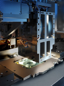
Teron 600 at work inspecting a reticle with 193nm light. The large NA objective is visible below the 6” square mask (source: KLA-Tencor).

Teron 600 at work inspecting a reticle with 193nm light. The large NA objective is visible below the 6” square mask (source: KLA-Tencor).

There are now three plausible lithography paradigms for the 2Xnm generation: EUV, pitch-splitting double patterning (PSDP) with immersion 193nm exposure, and wet 193nm with source-mask optimization (SMO) and other tricks. Thus it is not enough to inspect reticles with the same actinic wavelength as today’s immersion scanners. Additional defect categories must be detected and complex wafer-plane modeling adopted to evaluate their impact, according to Lopez. The Teron 600 platform (see figure) is thus intended to detect defects on all types reticles proposed for the 2Xnm generation, whether they will be printed with transmitted 193nm or reflected EUV radiation, and is designed to be extendable for future shrinks.

Other reticle defect inspection tools have employed sub-200nm radiation, but not in the same way as the industry-standard 257nm tools. In particular, the Applied Materials Aera2 and Zeiss AIMS systems have emulated the excimer illumination and reticle-side numerical aperture of exposure tools, while projecting an enlarged wafer-like image for analysis. Anomalies in that image directly relate to defects that appear on a developed chip, but do not indicate what caused those anomalies. The Teron 600 (and KLA-Tencor’s TeraScan systems) image the photomask with a high numerical aperture objective in transmission and reflection to capture the structure of the photomask at maximum possible resolution, finding numerous anomalies, many of them too subtle to affect wafer CD.

Photomasks no longer look like the target wafer patterns. For the 3Xnm and 2Xnm nodes, computational lithography techniques such as Inverse Lithography Technology (ILT) and Source Mask Optimization (SMO) produce fractured geometries with an enormous number of very small features, making the masks difficult to manufacture. In PSDP, not all the edges that define the CDs of a circuit layer are on a single mask, necessitating multilevel database processing and context sensitive defect detection to deal with “mask to mask” (M2M) defectivity. To reject the nuisance defects, the Teron 600 employs computational lithography methods in real time to simulate the pattern at the wafer plane. Resist response and – for SMO – the complex programmed illumination distributions must be included in the model in order to correctly evaluate the yield impact of detected anomalies. If the computation indicates that an anomaly is likely to cause an unacceptable CD excursion, reticle plane images are available to suggest repair strategies to the user.

“EUV reticle inspection is actually the most straight forward,” claimed Lopez. “The key requirements are high resolution inspection in the reflection mode and low-noise imaging in an ultra-clean environment.” With a 55nm pixel size, the capability of finding programmed defects in multilayer reflector topography down to 2nm height and <40nm diameter and to model EUV illumination effects, the Teron 600 is ready for first-generation EUV reticles, claimed Lopez. Low noise results from the use of an innovative, quasi-CW 193nm laser system. Lopez reported that KLA-Tencor has more than 10 lasers from its secret overseas supplier, and some have operated for 2 years in the lab.

The Teron and TeraScan platforms are compatible, facilitating a mix-and-match capacity optimization strategy and effective integration of data from critical and non-critical layers, according to KLA-Tencor. The Teron 600 is reported to have successfully inspected 30 highly secret prototype reticles created for source-mask optimization / inverse lithography technology, double-patterning lithography, and EUV (both patterned masks and blanks). The tool comes in two configurations, depending on whether the user wants a 3- or 4-hour turn around time for inspection. The first beta test tool is being shipped now, leaving 4 more being tested at the KLA site. Lopez estimates that roughly 10 high-end mask shops will need the Teron 600 for near term development. Since it can be applied to all projection lithography reticles currently being investigated, no technology commitment need be made, except, perhaps, not to emphasize imprint lithography. – M.D.L.

Friday, September 18th, 2009

At SEMICON West this year, ASML announced tools that fleshed out their Holistic Lithography scheme introduced at SPIE’s Advanced Lithography Symposium in February of this year. The key idea of Holistic Lithography, according to Bert Koek, senior vice president of the applications products group at ASML, is integrating computational lithography, wafer printing, and process control to enable shrink towards 32nm using 193nm water immersion exposure tools. The computational facet reduces the process window shrinkage, advanced tooling enables volume manufacturing, and new metrology methods insure that the tools remain centered on the process window.

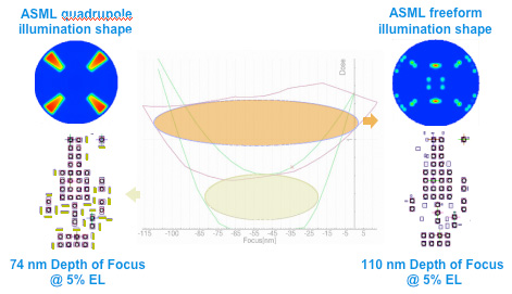
The same contact hole pattern (lower right) can be printed with improved process window (center) using FlexRay illumination (upper right) than with quadrupole illumination and a mask with sub-resolution scatter-bars (green). (source: ASML)

The same contact hole pattern (lower right) can be printed with improved process window (center) using FlexRay illumination (upper right) than with quadrupole illumination and a mask with sub-resolution scatter-bars (green). (source: ASML)

The Tachyon Source-Mask Optimization announced in February addressed design issues by incorporating a software model of the exposure tool in the OPC/illumination optimization process. Specific tool tuning knobs could be set to optimize the process window for key design clips. The illumination geometry, however, was constrained to what could be implemented with diffractive optical elements, which had to be ordered, fabricated, and delivered along with the mask. The FlexRay illumination system, announced at West, replaces the diffractive element with a micro-mirror array of 4000 elements (see figure), each of which could be set independently in near real time. That allows more complex illumination schemes which can be matched to the actual tool and delivered reticle. According to Koek, free-form illumination enables larger process windows with simpler OPC schemes (see figure), reducing mask costs. “The idea is to push the complexity from the mask to the illumination source, which is purchased only once,” said Koek. Free-form source tuning can also correct wafer CD biases due to mask fabrication realities, while maintaining OPC validity, claimed Koek.

Once the best process window is achieved, the challenge becomes preventing the exposure tool from drifting away from optimum conditions. The new ASML BaseLiner scanner control system insures optimum critical dimension uniformity (CDU) and overlay without maintenance actions that interrupt production. Instead, single monitor wafers are exposed once or twice a day and analyzed using ASML’s not-so-secret YieldStar scatterometry system, which determines corrections that can be implemented using control “knobs” on the scanner. By measuring 4000 targets on the monitor wafer offline, YieldStar (supplied as part of the BaseLiner scanner stability package) simultaneously calibrates focus, dose, and overlay. Koek showed data in which this system resulted in a 3X improvement in ASML’s 1900i tool overlay to <5nm over 1 month.

ASML offers its various Holistic Lithography products and services as Eclipse packages, optimized for node, layer and process. Not all manufacturers will want to use the new ASML products for all the functions, so Eclipse assembles those needed as blocks with the option to interface with existing tools and processes. As the industry approaches the limit of water immersion lithography, intelligent integration of wafer lithography, computational lithography and process control will become crucial. The ASML Eclipse system with its hardware and computational features integrated holistically into production, potentially offers one way to continue shrinking devices with acceptable yield. –M.D.L.

Wednesday, September 9th, 2009

After more than 5 years and US$500 million dollars invested, Nanosolar has emerged from secrecy to quell rumors that the company’s technology was all smoke and nanomirrors. This long-shot technology risk is now claimed to produce mean cell efficiencies of 11%, with a champion cell from a Gen3 line measured by NREL at 16%. The use of dual-laminate aluminum foil with metal-wrap through (MWT) back-contacts reduces costs while allowing for improved electrical output. The company claims >US$4B in order backlogs, though the first MW-scale installation is only now in the works.

The world has long known that Nanosolar has been trying to achieve medium efficiency (10-15%) PV technology with an order of magnitude reduction in fab costs compared to thin-film PV leader First Solar’s CdTe on glass single-substrate approach. Using aluminum foil in roll-to-roll (R2R) continuous processing allows for printing-press-like costs, and the substrate itself can be the bottom electrical contact. In contrast, Ascent Solar uses a flexible plastic substrate for R2R CIGS fabrication.

The nano-ink formulation, the ink printing, and the rapid-thermal processing (RTP) technology (see figure) needed to form 10-15% efficient CIGS cells is the crown jewel in Nanosolar’s IP crown. Other companies may use R2R and printing presses and clever cell contacts, but no other company has invested in CIGS nanoparticle ink technology like Nanosolar to create an inexpensively printed yet high-quality semiconductor.

Prior to working internally to develop the nanoink in 2003 and 2004, Nanosolar investigated a broad range of avenues for printed CIGS. This included chemistries and processes based on partial-oxide spray pyrolysis (for which the company licensed patents US 6,268,014 and US 6,821,559); metal oxides (discarded due to long oxide reduction required and difficulty of including Gallium); organometallic precursors (discarded due to high cost); solid-solution nanoparticles (for which the company licensed US 7,091,136 and US 7,521,344); metal hydroxides and metal salts (US 2008/0280030); hydrazines (discarded due to lack of manufacturability, with many coat/anneals required and hydrogen selenide generated); and high throughput 3D-ALD (US 7,115,304).

The MWT back-contacts look like they borrow IC packaging substrate technology ideas. Vias are drilled (not specified, but are likely to be cut by lasers) through the CIGS and associated thin-film layers using a single tool capable of supporting hundreds of MW of annual capacity. The cell foil is laminated with a secondary low-cost aluminum foil with an insulating adhesive in between. Insulated holes are filled with a conductive paste to create a conductive via (see figure). MWT cell architecture provides for cells capable of generating and carrying currents of 6-25 Amps, which is claimed to be 3-10x more than is cost efficient with other thin-film PV technologies.

Nanosolar must be commended for showing the most sensitive of all fab data: process stability over time. The company’s white paper includes the efficiency numbers tested for 150 cells from a single roll (see figure) processed on August 29 of this year at the fab in San Jose. While there are clearly five cells with <4% efficiency, and another five in the 4-8% range, the MWT Gen2 process seems to be under control with average efficiency of 11.75%.

The company claims to have developed five incremental generations of R2R processing tool designs between 2005 and 2008. Along with faster rolling speeds, the roll width has been increased from 100mm to 750mm, and 1500mm width processing has been demonstrated. Most of the process steps are non-vacuum, and thus inherently relatively easy to scale up. One of the current largest roles is equivalent to 100kW of PV power, which would be the equivalent of 1,000 glass plates.

Panels are assembled at Nanosolar’s fully-automated line in Germany, where one panel can be produced every 10 seconds. Full 24/7 capacity is claimed to be 640 MW/year of panels. The company claims to have over US$4B in order backlog; though all activity is dependent upon commercial banks for financing. –E.K.

Wednesday, August 26th, 2009

IMEC/F-IZM/SUSS/TM vs. SEMATECH/Leti/EVG/Brewer.

The leading R&D consortia have aligned (pun intended) with leading equipment and materials suppliers to create ultra-thin silicon wafer handling technologies for 3D ICs. With the ability to shrink circuit dimensions in 2D becoming ever more difficult, most of the world’s IC fab leaders are evaluating the use of the 3rd dimension. In addition to the EMC3D suppliers’ consortium, all of the leading IC technology R&D consortia (IMEC, Fraunhofer-IZM, Leti, and SEMATECH) now have 3DIC programs in place with equipment and materials suppliers.

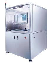
IMEC and SUSSMicroTec recently started a joint development program. Together, they will develop permanent bonding, temporary bonding and debonding processes for 3D system integration, including through-silicon-via (TSV) manufacturing. IMEC will use SUSS ’s XBC300 production wafer bonder platform (see figure) to develop 200 and 300mm permanent metallic interconnect bonding, as well as temporary bonding and debonding solutions for its 3D-stacked Interconnect and 3D Wafer Level Packaging technology. The bond cluster also includes a spin coater, a low force bonder and a plasma chamber. The XBC300 temporary bond configurations are available for development and high volume needs.

For its 3D IC technology, IMEC uses a process flow where TSVs are realized in a single-damascene process that is performed immediately after active-device and contact processing but prior to formation of interconnect metallization layers. This process enables small via diameters of 1–5micron. After completion of the back-end wiring, silicon is removed from the bottom of the substrate to open the buried TSVs. Dice or wafers subsequently are stacked and interconnected in a wafer bonding step.

“We are very pleased to co-develop with SUSS MicroTec the processes for permanent and temporary wafer bonding for our 3D technologies,” said Eric Beyne, Program Director of IMEC’s Advanced Packaging and Interconnect Research Centre. “In particular, the debonding and handling of very thin wafers ranging from 25 to 50 µm is an especially challenging and critical process. We are convinced that the versatility of the SUSS wafer bonding and debonding tool platform will contribute to bringing 3D integration technology to maturity.”

SUSS’s XBC300 production wafer bonder is matched with material from Thin Materials (company in stealth mode) to create the temporary bonding solution to be used for challenging thin wafer handling. This material is capable of handling wafer processing temperatures in excess of 250°C, but can be de-bonded  at room temperature. Fraunhofer-IZM works with the team at Thin Materials, too.

“Thin Materials’ technology for temporary bonding perfectly complements our process offering portfolio for 3D Integration and Packaging”, confirms Frank Averdung, President and CEO of SUSS . “Partnering with Thin Materials allows us to offer our customers a wide variety of temporary bonding technologies according to their specific needs.” Together with its partners 3M, Disco, DuPont, NEXX Systems, Surface Technology Systems, and Thin Materials, the company hosted a TSV 3D Integration workshop introducing solutions for temporary bonding and thin wafer handling on July 15th during SEMICON West.

Meanwhile, CEA-Leti continues to work with EVG and Brewer Science on temporary bonding for 3D ICs. Thorsten Matthias, director of technology for EVG North America, presented “Thin Wafer Handling and Chip Stacking for 3D Integration” at the SEMICON West Test, Assembly & Packaging TechXPOT.

SEMATECH has purchased an EV Group wafer bonder with “SmartViewNT” technology (see figure) for TSV wafer-to-wafer (W2W) bond alignment. The alignment uses a high-precision stage that comprises top- and bottom-side microscopes to ensure the highest degree of accuracy for all types of alignments, including face-to-face, backside and infrared-transparent. Initial results for W2W alignments demonstrated <0.3 µm face-to-face alignment accuracy, eliminating the need for post-processing steps such as generating backside alignment keys.

“We’re seeing a pivotal shift in the industry, where equipment suppliers and research institutions and universities alike are beginning to rally together and work in greater collaboration in preparation for when the market rebounds,” said EVG vice president and general manager, North America, Steven Dwyer. The company claims an increase in orders for pilot line production service, indicative of widespread industry interest in 3D.

EVG and Applied Materials are working together as part of EMC3D on wafer-bonding processes for stacking using TSV. As reported by BetaSights in April 2009, Applied Materials is working with Disco on wafer thinning. Disco is working with SUSS. Nonetheless, SUSS  and EVG are still strong competitors and are NOT working together.

Olympus Integrated Technologies America, Inc. (Olympus-ITA) has provided an infrared (IR) inspection and defect review system (see figure) with metrology software to SEMATECH for its 3D R&D Center at the College of Nanoscale Science and Engineering’s (CNSE) Albany NanoTech Complex. The system—installed and accepted in April, 2009—enables SEMATECH to verify alignment of bonded wafers and TSV. “We have been collaborating with SEMATECH on inspection and defect review tools since 2001 and working with the 3D group since last year to provide a method to image and measure overlay offsets after wafers have been bonded together,” said Olympus-ITA president Greg Baker.

With so many alliances developing so many technologies, there were so many events during SEMICON West 2009 that it seemed impossible to attend them all. Fortunately, one of the more interesting events was recorded and archived. A panel discussion held both live (for an hour during SEMICON West) and in virtual space (for three weeks, shown as part of PR agency MCA’s “BrightSpots” 3D IC Forum, with excellent text and multimedia links still available online) brought together representatives from SEMATECH, Synopsys, Yole Developpement, EVG, and Terrazon Semiconductor. Paul Lindner, EVG’s executive technology director, offers his viewpoints on the role of wafer bonding and thin-wafer handling with Bob Patti, CTO of Tezzaron, chiming in from the manufacturing side (see YouTube video).

The BrightSpots 3DIC forum was moderated by Francoise van Trapp, formerly an editor with Advanced Packaging magazine, and now working with ex-SEZ technology executive Leo Archer on web-based 3Dincites.com (rhymes with “3D in-sights”). There’s no doubt that 3D is one of the most important technology concepts in ICs today, so it’s great that veterans like Trapp and Archer are working to provide a continuous source of information about this vital direction. –E.K.