Monday, November 8th, 2010

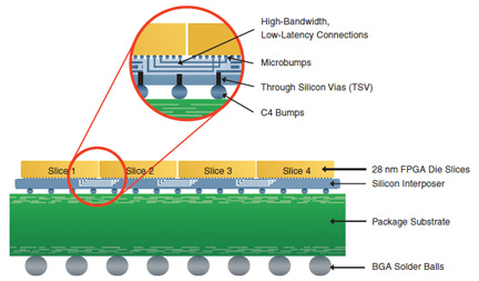
Xilinx has found the first major commercial IC fab problem which through-silicon vias (TSV) can solve: barrier-to-entry for large FPGAs and pseudo-SoC chips. BetaSights recently covered TSV technology pushed as a “solution looking for a problem,” and forecast use of TSV in silicon-interposers (“2.5D”) as the only significant near-term commercial volume. Ed Sperling at Chip Design recently covered TSV technology pulled as part of 3D stacking for 28nm and below chips. For Xilinx’s 28nm node Vertex-7 product, TSMC will use a 65nm node fab line to form TSV in silicon interposers along with multi-level-metal (MLM) interconnects.

Xilinx uses passive silicon-based interposers, microbumps, and through-silicon vias (TSV) for its 28nm node 7-series FPGAs (Source: Xilinx)

Xilinx uses passive silicon-based interposers, microbumps, and through-silicon vias (TSV) for its 28nm node 7-series FPGAs (Source: Xilinx)

The device is made using micro-bump assembly and a special FPGA architecture to match the interposers (figure). The multi-chip device delivers lower levels of power consumption, system cost, and circuit board complexity compared to using multiple FPGAs, each in their own package, for the same application. “Compared with traditional monolithic FPGAs, multi-chip packaging approach is an innovative way to deliver large-scale programmability with favorable yield, reliability, thermal gradient, and stress tolerance characteristics,” said Shang-yi Chiang, senior vice president of R&D at TSMC. Specs include up to 2.4Terabits/sec I/O bandwidth and 4.7 TMACS DSP performance.

Data flows between the FPGA dice and the interposer through more than 10,000 routing connections, providing over 100X the die-to-die connectivity bandwidth per watt at one-fifth the latency compared to prior multi-chip packages, without consuming any high-speed serial or parallel I/O resources. Xilinx claims that TSMC’s 28nm HPL (high-performance, low-power) process technology for the base FPGA device provides a comfortable power budget in the package.

Xilinx positions the 2 million logic cells possible in the device as extending the range of applications which can be addressed by an FPGA. “Our stacked silicon interconnect packaging approach makes this remarkable achievement possible,” said Vincent Tong, Xilinx senior vice president. “Five years of Xilinx research and development coupled with industry leading technology from TSMC and our assembly suppliers has made possible our efforts to provide an innovative solution…” The device targets next generation 100GE line cards, 300G bridges, Terabit switch fabric, 100G OTN muxponder, RADAR, and ASIC emulation.

Integration benefits of TSV interposers

“The Virtex-7 2000T FPGA using stacked silicon interconnect technology is a significant step in FPGA evolution and will enable ARM to implement the latest cores and platform solutions within a single FPGA. This will reduce our development effort, reduce power, and improve performance compared to a multi-FPGA approach,” said John Cornish, EVP and general manager, System Design Division, ARM. “We have been a long time user of the Virtex FPGA technology in the ARM Versatile Express SoC prototyping solutions and this will surely extend our strong position.”

Rolf Aschenbrenner leads Si-interposer work at Fraunhofer-IZM

Not specified by Xilinx but generally known is that silicon-interposers easily incorporate passive circuit elements such as resistors, capacitors, and inductors. If you have already committed to the integration expense of interposers for other reasons, then you almost certainly will want to take advantage of ability to integrate passives. All Silicon Systems Integration Dresden (ASSID) program within Fraunhofer IZM works on Cu-TSVs with diameters in the 2-20 ?m range, and on functionality extensions of 300mm silicon interposers with passives. Rolf Aschenbrenner (figure) has recently been appointed as the deputy head of Fraunhofer IZM, and co-head of the Systems Integration and Interconnect Technologies department.

Time-to-market for both large FPGAs and FPGA-based SoCs should be improved by the use of TSV-interposers. Xilinx claims it was challenged by some of it’s customers to be able to supply high-volumes of 2M-gate FPGAs almost immediately after the start of production, when line yields are still low. Modeling showed that early line defect levels would kill most 2M-gate chips but most 0.5M-gate chips would yield, so combining four of the latter using a high-bandwidth silicon-interposer will allow the functionality to reach market much faster. Xilinx is now proving software design support to beta customers, and initial devices will be available in the 2nd half of 2011.

Vertex-7 designs are available as part of “EasyPath-7” software, allowing portability to lower cost while lower performing FPGA families. The Artix-7 familyoptimized for lowest power and lowest cost using wire-bond chip-scale BGA packagingaddresses cost-sensitive, high-volume markets like portable ultrasound, digital camera control, and software defined radio. The Kintex-7 family optimized for low power signal processing using BlockRAM and DSPis for wireless LTE infrastructure equipment, LED backlit and 3D digital video displays, medical imaging, and avionics imaging systems.

On November 16, the San Francisco Bay Area (SFBA) Nanotechnology Council Chapter of the IEEE is hosting a ½-day symposium next week on “Nanoelectronics: Innovation and Implementation” that will include a presentation by TSMC vice president of technology applications Di Ma on “Technology Challenges in 28nm CMOS and Beyond.” GloFo and Samsung will also give presentations at the event, which will be held on National Semiconductor’s campus in Santa Clara. Stay tuned for more news on 2.5D ICs. –E.K.

Monday, October 18th, 2010

The International Electronic Devices Meeting (IEDM) this year—the 56th annual meeting, to be held December 6-8, 2010 at the Hilton San Francisco Union Square—will include presentations on alternate channels and multiple gates for CMOS transistors at the upcoming 22nm node. While dual- and tri-gate CMOS transistor devices have been shown for many years, proven single-gate silicon technology has been extended with strain and high-k metal-gate (HKMG) options. Now, with transistor structures such as HKMG reduced to single atomic layers, the next performance boost will likely come with alternate channel materials and the possible use of dual-planar gates.

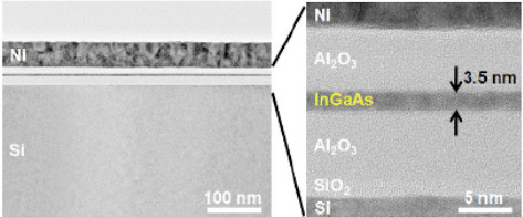
A team led by University of Tokyo wafer-bonded InGaAs alternative channel material to silicon to form dual-gate MOSFETs on an insulating substrate. (Source: IEDM 2010)

A team led by University of Tokyo wafer-bonded InGaAs alternative channel material to silicon to form dual-gate MOSFETs on an insulating substrate. (Source: IEDM 2010)

The limits of the single-gate bulk silicon CMOS transistor seem to be upon us, despite extensive use of strain and other clever extension tricks. For 22nm node devices, there is excessive variability due to channel doping variations (<100 dopants atoms per channel), gate leakage, and parasitic capacitances. Such issues have been known for years, and researchers have developed various known ways forward, including the use of a silicon-on-insulator (SOI), alternate materials for the channels such as germanium (Ge) and indium-gallium-arsenide (InGaAs, figure), as well as dual- and tri-gate transistors.

So far, SOI has been used by IBM and AMD for microprocessors and by all video game makers for the main brains in their boxes, but there is major additional cost for the substrate and so most commercial fabs do not run SOI wafers. Multiple gates have been pushed out again and again. Trigate transistors—a.k.a. “finFETs” and many variant names for their cross-sectional shapes—have long offered superior performance for minimal additional cost, but EDA models didn’t exist for such devices and so it was difficult to design them into commercial ICs. Now these technologies are under consideration for high-volume use in the next few years, as will be shown in presentations at IEDM 2010.

Fully-depleted SOI (FDSOI) is claimed by CEA/Leti/Minatec [Session 3.2] to be easier to integrate than non-planar devices like finFETs. This paper will address electrostatic integrity, drivability, within wafer variability, and scalability with silicon data down to 18nm gate lengths. Solutions to the challenge of multiple VT transistors and non-logic devices (ESD, I/Os) will also be reported.

Dual-gate FDSOI work-function control to tune multiple VT levels will be shown by CEA/Leti/Minatec along with ST, Soitec, and Aixtron [Session 3.4]. By work-function engineering of TiN/TaAlN metal gates, short channel performance of 500µA/?m ION and 245?A/?m IEFF at 2nA/?m IOFF and VDD=0.9V will be reported on pMOS with a TaAlN gate. The combination of two metal gates with either n- or p-doped ground planes below the Ultra-Thin Buried Oxide (UTBOX) can offer 4 different VT from 0.32V to 0.6V for both nMOS and pMOS. Most of the same researchers will later show [Session 11.2] high-performance planar multi-gates devices with a Si-conduction channel of 4nm, allowing drive current up to 1350µA/µm @Ioff=0.4nA/µm. Vitally, this paper will also show how to self-align the two planar gates, based on, “the direct exposure of a HSQ layer through a 5nm Si-channel.” This opens the way to an easy planar multi-gate process for ultimate CMOS, fully co-integrable with conventional devices.

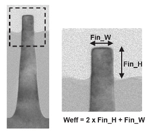
SEM cross-section of finFET from TSMC's complete high-performance 22/20nm CMOS logic technology, featuring SiGe stressors, metal gates, and high-k dielectrics. The FinFETs were used to build a dense 0.1µm2 SRAM memory cell. (Source: IEDM 2010)

SEM cross-section of finFET from TSMC's complete high-performance 22/20nm CMOS logic technology, featuring SiGe stressors, metal gates, and high-k dielectrics. The FinFETs were used to build a dense 0.1µm2 SRAM memory cell. (Source: IEDM 2010)

FinFET architectures will be shown twice by TSMC to be ready for 22nm node fabrication [Sessions 27.1, 34.1]. The company will present on a high performance 22nm bulk finFET (figure) that achieve “best-in-class” Ion of 1200(N)/1100(P) uA/um for Ioff=100nA/µm at 1V. Dual-Epitaxy and multi-stressors are essential to boost the performance of dual workfunction HKMG transistors. The company’s abstract claims that finFETs, “the transistor architecture of choice for high performance CPU applications, can also be extended for general purpose SoC applications by proper device optimization.” For low-operating power applications, significant Ion improvement and Ioff reduction are claimed through EOT scaling and mobility improvement. N-finFET and P-finFET achieve ION of 1325 µA/µm and 1000 µA/um at 1 nA/um leakage current under VDD of 1 V, respectively.

Due to ever increasing complexity and cost, the real details of next-generation fab processes are generally kept secret. Even when discussed, there is always the possibility that the information presented is a dead-end with hidden problems. Novel technology may work, but may come with unacceptable side-effects like cost increases and yield losses. Managing the complexity of process technology interactions, and knowing which processes to deploy at the right time establishes the typically slow pace of evolution.

So finFETs remain attractive but are probably more challenging to integrate compared to alternate channel materials, and unless TSMC has made a big hidden investment in EDA modeling they probably cannot be designed into mainstream 22nm node ICs. Planar dual-gates are probably the best bet for the next major transistor architecture, so long as a self-aligned approach can be made to yield well. However, even dual-gates may be pushed out past 22nm, since alternate channel materials will likely be used at 22nm and should provide sufficient performance. If so, then the 16nm node would be the first use of dual-gates with or without FDSOI, and finFETs would be pushed out indefinitely.

The best way to understand this complexity is to attend IEDM and talk to the manufacturing folks who have to make it happen one way or the other. If you cannot attend in person, the conference organizers have created a page on Facebook, and they will be posting tweets to Twitter including paper titles and links to the technical program sessions. IEDM also includes the latest and greatest presentations on power electronics, memory cells such as Flash and upcoming ReRAM, RF and ultrafast ICs, CMOS image sensors (CIS), and devices results using everybody’s current favorite sticky-tape-your-way-to-a-Nobel-Prize-material graphene. A plenary talk entitled “Energy Efficiency Enabled by Power Electronics” will be given on the first day by Arunjai Mittal of Infineon Technologies. Stay tuned. E.K.

Tuesday, October 5th, 2010

The mask making community, comprising the BACUS technical group of SPIE, has had a fraught relationship with maskless lithography. On the one hand, the most lucrative part of the mask-making business would vanish if massively parallel e-beam direct-write (EbDW) lithography displaced DUV or EUV to take over the leading edge. On the other hand, before that happened, the difficulty and cost of mask-making would drop precipitously, motivating an expansion in the number of designs and hence mask sets. The 2010 BACUS/SPIE Symposium on Photomask Technology in Monterey, CA, held an all-day session evaluating the prospects of Maskless Lithography on September 15.

The prospects are not great, even for a limited role in prototyping or line-end cutting for gridded chip designs. Stefan Wurm of SEMATECH summarized the difficulty: maskless is not on track for insertion at the 22nm node. Full system demonstrations at specified resolution and throughput would need to be on the horizon right now. Instead, there are a variety of pre-alpha prototypes illustrating the difficulties of a massive technology shift (figure). Rather than insertion into high-volume manufacturing, Wurm advocated an application of massively parallel e-beam technology in mask-writing. Even that, however, would require an investment of $300M or so that the industry does not have available.

Tor Sandstrom of Micronic Laser Systems discussed two unaddressed problems: the bandwidth needed to send data into a writer capable of printing a practical number of wafers, and the need for 100% functional inspection because of the finite probability of isolated data transfer errors. To print 100 wafers-per-hour at the 16nm node, Sandstrom estimated that the pixel transfer rate would have to be 160 terapixels/second (Tp/s) for gray-scale writing or 420 Tp/s for binary writing. That corresponds to 150 times the data processing capacity of the Large Hadron Collider in Geneva, or a large building full of top-of-the-line Cisco routers, or ~10 million HDTV channels! As amazing as that demand may seem, it is theoretically within the capability of today’s fiber optics.

With any plausible bit error rate, there would be anomalies somewhere on every chip, necessitating inspection. However, what do you inspect? A real-time data driven system has vastly more defect modes than today’s DUV printing with perfect masks. Statistical inspections will not do, only full functional tests would be reassuring, and that is impossible, according to Sandstrom. Some means of multiple writing, voting and error reporting has to be implemented, complicating the system and slowing throughput. “Maskless lithography is not for the faint hearted,” summarized Sandstrom.

Neil Berglund of the Northwest Technology Group analyzed costs under various throughput conditions and found some niches where maskless lithography might be economical. However, he pointed out that in a massively parallel e-beam system, every beam had to work the same all the time. If there were more than one exposure tool, the difficulty of perfect tool matching would require “lot-to-tool dedication” where every exposure on a lot of wafers would be made on the same tool. The logistics of that would extract a cycle time penalty that might overwhelm any mask-less advantage.

The developers of massively parallel e-beam write tools all reported progress, with MAPPER (which has delivered two 110-beam pre-alpha tools to strategic customers) probably furthest along towards manufacturing. However, Bert Kampherbeek, VP of Systems Engineering at MAPPER, was fully aware of the challenges remaining. The goal remains a 10 wph tool at a cost below 5 million Euros and a footprint of 1 m2, to allow clustering. Getting there means getting all 13,000 beams up, boosting the total beam current to 160 uA on the wafer, rather than today’s picoamps, and lots of system integration.

Mark McCord of KLA-Tencor revealed breakthroughs made in their DARPA-supported reflective e-beam lithography (REBL) tool which uses a reflective pattern generator chip rather than a transmissive MEMS blanker array. KLA-Tencor has replaced the massive “magnetic prism” which separated the source and patterned beams with an elegant Wien filter and placed a channel plate micro-lens array next to the pattern generator chip to deal with fringing fields. The net result was to shorten the e-beam column to ½ meter, which allows 2.75 uA to be delivered to the chip at <45nm resolution. The 50kV, 62.5X demagnification architecture images 8 pattern generator pixels on each wafer pixel, reducing the effects of errors and anomalies. The pattern generator chip has a 248×4096 pixel array on a 1.6 um pitch, each pixel controlled by 11 transistors. Six wafers are printed simultaneously using a million beams on a continuously rotating maglev stage, with the pattern generator image following the motion of the wafers. Printing with 32 grey-scale levels allows proximity correction as well as on-the-fly error correction. The pixel pitch of 26nm has been resolved, suggesting that the DARPA goal of 45nm resolution is within reach. However, the industry needs 16nm and >10 wph. Because of Coulomb’s law, tightening resolution in e-beam lithography implies reducing beam current and throughput. Still, adding more pixels or columns could take the innovative REBL architecture far enough.

Other vendors described less radical options. Matthias Slodowski of Vistec promoted their multi-shaped beam (MSB) system. This scheme leverages the standard variable shaped beam (VSB) architecture where a flood electron beam is steered through two rectangular apertures which shape it to produce various rectangular geometries in the exposure. Vistec’s evolutionary proposal is to replace each pair of apertures with an 8×8 array, with 64 beamlets steered and shaped independently. A proof of lithography tool has worked with 16 beamlets to pattern 45nm node contact arrays. That could be enough for mask making. Akio Yamada of Advantest described their cell-projection direct write system, which is already being used in the short-turn around wafer shuttle program. With proper design for e-beam (see previous eBeam Intiative article), such systems could form a bridge to whatever comes after 32nm.

An audience member from a major semiconductor manufacturer lamented the dis-integrated and under-funded nature of the maskless lithography effort. His company wanted to use maskless lithography, but needs several complete manufacturing systems, not a bunch of disconnected projects on beam-shaping, data path, verification, etc. Established semiconductor equipment manufacturers need to take over the field and deliver qualified systems to customers, in his opinion. Big companies need two reliable sources of such critical equipment, but he did not yet see two capable companies stepping up. Without semiconductor equipment industry buy-in, the best outcome would be some orphan prototype tools, which might be tried at a few major mask companies or R&D consortia. That would not lead to a solution to the coming crisis for innovative companies and short production run chips. – M.D.L.

Thursday, September 23rd, 2010

Through-silicon vias (TSV) have been in R&D for over 10 years, and finally may reach commercial use in IC manufacturing next year. However, instead of forming vias through silicon in ICs (TSV-IC), the near-term needs will be for vias though silicon interposers (TSV-interposer) made in outsourced test assembly and packaging (OTAP) fabs. Presentations at conferences including SEMICON/West, IMAPS, and IEDM in this year provide perspective on the slow evolution of this 3D IC technology.

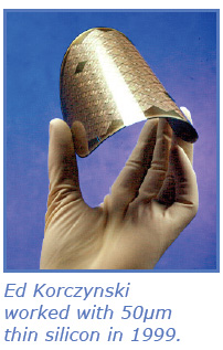
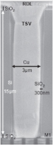
TSV has been a bit of a “solution looking for a problem” since first conceived. This editor worked on the technology in the years 1999-2000 for a startup called TruSi (now a TSV-interposer foundry called AllVia, to which this editor has no relationship), trying to sell an atmospheric pressure etch tool to do silicon thinning to 50µm (figure) and below. Despite continued interest in TSV capabilities, a viable (pun intended) “problem” was always lacking. Nonetheless, the entire industry ecosystem of original equipment manufacturers (OEM), specialty materials suppliers (SMS), and consortia have continued to develop and push TSV technologies out into the world. In addition, there have always been “boutique” mil/aero companies like Vertical Circuits with 3D-IC IP looking to expand into high-volume commercial markets. The result is a confusion of options, and no real cost or yield data for volume manufacturing.

Perpetual pundit Phil Garrou—now blogging for PennWell’s “ElectroIQ” site after being tossed out with other editors when Reed closed Semiconductor International—reports that leading OSAT ASE is soon going to be ready with TSV-interposers. During OEM Suss Microtec‘s “3D IC Bonding and Thinned Wafer Handling Workshop,” at SEMICON/West this year, Calvin Cheung, vice president of engineering for ASE, said, “We currently need an interposer to bond 28nm low-k die,” he said. “Right now it is impossible to stack these mechanically unstable materials into a reliable 3D stack in any other way.”

Alchimer also held a workshop at SEMICON/West to show how it’s all-wet molecular deposition technology can reduce costs in any TSV fill step. During this workshop, Riko Radojcic, director of engineering at Qualcomm CDMA Technologies, said that, “We have certain form-factor constraints that may motivate us to use TSV.” The killer-app is video processing bandwidth in mobile devices, and, “if it will be 3D based on TSV or PoP remains to be seen…but it’s clearly not going to be served by routing through a PCB,” said Radojcic. For Qualcomm’s 3D circuits, the logic chip would be on the bottom with TSV-IC, while memory or analog would be on top as a flip-chip. “We focus on heterogeneous integration,” explained Radojcic, “not logic on logic stacking.” Qualcomm’s 3D stacks already have to manage power for other reasons, so any eventual TSV-IC would not need thermal vias.

(IEDM 2010, Session 35.1)

(IEDM 2010, Session 35.1)

The IMAPS 2010 conference scheduled for November 2-4 this year in Raleigh, North Carolina will include a special track on 3D packaging and integration [NOTE: early registration and hotel deadline Sept. 24]. One presentation will be on “Enabling robust copper fill of super high aspect ratio through silicon vias” by Novellus Systems. In an exclusive interview with BetaSights, Novellus’ senior director of business development for 3D applications Damo Srinivas confirmed that interposers appear to be the main near-term TSV volume, and so the final silicon target thickness will be 100-140µm.

Interposer thickness cannot be reduced below 100 microns without rigid silicon wafers becoming flexible silicon foils. Typical TSV processes to date have worked with 5:1 to 10:1 AR, which may be acceptable for TSV-IC that could be 10-50µm thick. However, 10-20µm diameter TSV consume too much silicon area, and take too long to etch and fill. Novellus has integrated a low-temperature vapor deposited dielectric, Cu barrier/seed vapor deposition, Cu electroplating, and Cu overburden wet-etchback in 20:1 AR TSV 100µm deep. Novellus has also claimed that proper integration of the barrier/seed and ECD steps allows for control of the Cu grain orientation inside TSV, such that post-anneal protrusion can be reduced from 0.8 to 0.2 µm, and at IEDM 2008 protrusion was shown by IBM to increase contact resistance.

TechSearch International has recently published a market forecast for silicon interposers, as part of the company’s Advanced Packaging Update Service.

Some day the world will probably need TSV-IC for mainstream commercial chips. To that end, the 56th International Electron Devices Meeting (IEDM 2010) in San Francisco, California, December 6-8, will include a presentation on TSV-IC titled, “Investigation on TSV impact on 65nm CMOS devices and circuits.” French researchers put 4µm diameter TSV through 65nm node ICs (figure), and for the first time experimentally quantified an electrical coupling between TSVs and MOSFETs. This coupling induced a spike variation of up to 7 µA/µm on the static NMOS drain current, though ring oscillators nearby were reportedly not effected. –E.K.
Tuesday, September 14th, 2010

Electron-beam (e-beam) lithography has long printed the photomasks used for chip production, but conventional vector-scanned e-beam tools will take too long to write the highly complex structures needed for the 22nm node if they have to be exposed using 193nm immersion (193i) lithography. That puts mask-makers in the same bind as chip-makers who have craved higher throughput in e-beam direct write (EbDW) lithography. Now, some of the innovations developed for direct write chip production are being applied to mask-making, as revealed at the SPIE/BACUS Photomask Symposium, today in Monterey, California.
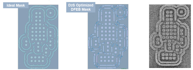
The trick, according to Aki Fujimura, CEO of D2S and managing sponsor of the e-Beam Initiative (figure), is design for e-beam (DFEB) along with cell projection e-beam exposure tools. In the cell projection, the e-beam column is equipped with shaped apertures that match typical wafer or mask geometries so that they can be printed in a single shot, rather than assembled from the rectangular shots of a conventional vector-scanned e-beam mask writer. DFEB encourages layouts that employ these pre-defined shapes to reduce the number of exposures needed for a mask or wafer. Using both methods can reduce the time needed to write a 22nm-node mask from ~80 to <30 hours, according to Fujimura. “The more complicated the mask is, the more we can help,” he stated in a pre-conference interview on Sept. 7.

The masks have gotten so difficult to produce because they have to be designed for manufacturing with 193i exposure tools, which have an intrinsic resolution limit of ~40nm. Obtaining an acceptable process window for features that size requires adding curvilinear sub-resolution assist features (SRAF) to the mask. The end result is that the 4X mask pattern becomes much more complicated than the chip, with minimum features of similar size. Applying DFEB to DFM masks is something of a revolution as it forces designers to confront yet another real-world manufacturing limitation.

The good news, according to Fujimura, is that DFEB can reduce the complexity of mask making by applying knowledge of the e-beam exposure process. Near the resolution limit of an e-beam exposure tool, the resist patterns are rounded and the exposures graded at the edge, just as they would be in optical lithography. Understanding the dynamics of e-beam exposure allows model-based fracturing with shapes overlapping rather than adjacent. Modulating the dose reduces the roughness of the edges without increasing the shot count. The net effect is faster throughput with better mask functionality, averred Fujimura.

An ideal ILT mask layout for a contact array fractured for printing mostly with circular beam spots and a DFEB optimized layout with fewer shots, finally an SEM of the resulting resist pattern on the mask. The contacts are meant to print at ~55nm diameter. (source: The e-Beam Initiative and JEOL)

An ideal ILT mask layout for a contact array fractured for printing mostly with circular beam spots and a DFEB optimized layout with fewer shots, finally an SEM of the resulting resist pattern on the mask. The contacts are meant to print at ~55nm diameter. (source: The e-Beam Initiative and JEOL)

Some of the advantages of DFEB mask technology had been presented at the 2010 Photomask Japan conference in April. Jeol has developed the JBL 3200MV, a mask writer with circular apertures to print round shapes and the capability to vary dose. The first example of an inverse lithography 22nm node pattern written with that tool showed a 30% shot reduction compared to a manhattanized fracturing and VSB exposure and showed better CDU (figure). At BACUS, the e-Beam Initiative reported another 17% shot reduction when DFEB methods had been applied to a manhattanized layout and printed with conventional VSB shapes. The net result is a 40% reduction in write time.

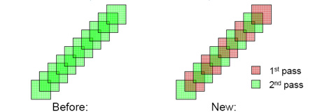
Printing a diagonal SRAF without, and with dose modulation using a square e-beam.

Printing a diagonal SRAF without, and with dose modulation using a square e-beam.

AIMS analysis showed the ideal and DFEB rectangular masks were functionally equivalent. Further throughput enhancement were predicted with dose modulation (figure); a curvilinear SRAF can be printed in two passes if each shot has ½ the dose, or with every other shot at full dose. That would reduce beam blanking time by 50% and speeds SRAF writing by 25%.

DFEB for masks speeds the printing of sub-30nm layouts that were previously unfeasibly complex. However, there is more to semiconductor mask-making than e-beam writing. Chips have to be designed, modeled, laid out, design rule checked, taped out, fractured, mask rule checked, written, inspected, re-written, and repaired… and then the mask set has to be accepted by the customer. The e-Beam Initiative is seeking buy-in from all participants in this complex ecosystem. All have secrets to keep. On September 7, 2010, the Initiative announced that 4 new player have joined the prior 30: Abeam Technologies, EQUIcon Software GmbH Jena, Synopsys, and TOOL Corporation.

The e-Beam Initiative has a considerable educational task ahead of itself if it is going to succeed in introducing DFEB masks at the 22nm logic node (HVM in 2012 or 2015). Fujimura reported that collaborative development is on-going now, with only a part being reported in the four papers presented at BACUS. Since no one can keep a mask writer working properly for 80 hours, one has to wish them well. – M.D.L.

Tuesday, September 7th, 2010

On August 31st, HP announced that it’s memristors and circuit-smarts will combine with Hynix’s manufacturing prowess to bring resistive RAM (ReRAM) chips to commercial markets in three years. HP Labs’ leader Stan Williams says that ReRAMs based on his team’s titania resistor should be able to switch 10x faster than 22nm node NAND Flash, and do so with 10x lower power consumption using unique circuit architectures and error-correction codes. HP’s corporate communications team worked to ensure that both mainstream and technology media reporters were briefed on this news, but most reports merely restate the press release. Refreshingly, Mark LePedus at EETimes provides the best overview of the non-volatile memory (NVM) marketplace, while ace technology reporter David Lammers freelances for the IEEE about the motivation for such a technology.

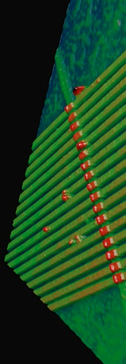
AFM image of 17 memristors formed at the titania cross points of thin nano-bars of platinum. (Source: R. Stanley Williams, HP Senior Fellow and Director, Information and Quantum Systems Lab, HP Labs)

However, only at BetaSights can you learn why HP leads with the materials engineering of memristors, how Stan Williams’ lab at HP has developed cross-bar architectures (figure) for ReRAMs over the last decade, and what issues remain to be solved before high-volume manufacturing (HVM) can commence at Hynix. This editor has toured the lab, and seen Williams present memristor details at Materials Research Society meetings, and the best source for technology information about memristors is still the April 22nd BetaSights post, Memristor manufacturing for memory, logic, and AI.” Go back and read it again, before continuing with this analysis of the deal with Hynix.

ReRAM work started at HP Labs ~2000, but it was only 2006 that the specific titania-based memristor device was found, and only in the last year or so that the non-electroforming PVD fabrication method was developed. As reported after the MRS spring meeting, many companies and universities are exploring memristor devices using other oxides besides titania that can be sandwiched between electrodes in cross-bar structures, but all other teams are still stuck with the need to use an expensive and unreliable electroforming step. Only HP has made the critical breakthroughs in both theory and practice that allow memristors to be formed inexpensively and reliably, and with IP protection for Ti4O7 PVD integration the company seemingly owns the only known way forward using titania.

Why do HP and Hynix think that it will take three years to move this from lab to fab? Well, the issues are not just integration and yield, but some of the most critical basic unit-processes may have to be completely re-done on Hynix’s R&D line. Deposition will almost certainly remain PVD for both electrodes and storage layers, since everything is planar and the process relies upon the stoichiometry tuning possible with PVD targets. However, the patterning to date has used a manual home-brew nano-imprint lithography (NIL) tool, and either a commercial NIL technology or a sidewall-spacer double-patterning (SSDP) approach will be needed for 300mm wafers. Also, the lab uses the ancient and messy technique of “lift-off” in a wet bath (note many defects in the figure), and some manner of dry etch will almost certainly be required for HVM yield. The etch of the platinum electrodes will be tricky, but there are known approaches using either SF6/Ar or O2/Ar plasmas.

The fast reversibility of 22nm titania memristors—due to the diffusion of oxygen-vacancies across just 1.2nm—is key to the many potential memory applications that could be served by ReRAMs. Many oxides and organics can be found that switch once for limited PROM applications, or switch slowly for niche NVM applications. Old technologies like MRAM and FRAM—both read as resistance changes—cannot function at 22nm due to the need to write cells with fields across larger plates. Phase-change RAM (PRAM, a.k.a. PCM, OUM, etc.) can be fast and tiny, but relatively more costly due to the need to integrate heaters and drive transistors.

We’ve heard about “ubiquitous” memory chips on the horizon many times before, and none have yet arrived. Only NAND Flash has even moved toward ubiquity by replacing HDD for a few niche applications, but while creating it’s own huge space in the mainstream it has failed to replace any established memory chip technologies. The clock is now ticking. If HP and Hynix are successful, the 22nm node memory market in 2013 will include ReRAM wafers made with costs and yields near Flash. If so, then the far superior densities and functionalities of memristors-based ReRAMs would result in a new leader setting the pace for Moore’s Law, and foundries (and maybe other memory IDMs) would have to see what the going price is for licensees. Terms of the JDA, such as how hypothetical licenses might be issued, have not been disclosed.

Besides ReRAMs, HP researchers have already shown that memristors can function as both 3D interconnect layers and latches for complex digital logic circuits. Researchers in Iran have discovered that two memristors in series precisely mimic the analog dynamics of human neurons, further justifying hope that learning circuits could finally lead to practical artificial intelligence (AI). Memristors now seem significantly closer to providing real fun and profit.–E.K.

Wednesday, August 25th, 2010

The IC fab industry is notoriously conservative, and normally abstains from risky behavior like contracting new processes. Still, there are times when what we’ve been doing no longer satisfies today’s needs, and we have to try something new. Both Novellus Systems and Applied Materials have recently announced new vapor deposition (VD) tools and integrated process recipes for silicon-oxide dielectrics, after many successful beta-site evaluations by customers. Both technologies create oxide films for 32nm and 22nm node device structures: transistor isolation, various integrated and sacrificial spacers, and sidewall spacer double patterning (SSDP) lithography. Both claim the ability to form “furnace-quality” films, with conformality somewhere between chemical-vapor deposition (CVD) and atomic-layer deposition (ALD).

CFD
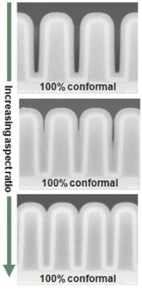
SEM cross-section of Conformal Film Deposition (CFD) into trenches. (source: Novellus Systems)

SEM cross-sections of Conformal Film Deposition (CFD) into trenches. (source: Novellus Systems)

Novellus Systems’ multi-station sequential processing (MSSP) PECVD Vector platform gets an upgrade to a new conformal film deposition (CFD) process capability. The company claims 100% step coverage on structures with aspect ratios (AR) of up to 4:1. The company shows SEM cross-sections of ideal trenches for deposition (smooth sidewalls <90°) that are nearly perfectly filled (figure). Such capability could meet 22nm requirements for front-end-of-line (FEOL) applications such as gate liners, spacers, and shallow trench isolation (STI), as well as the spacers that will be used for much of the world’s sidewall spacer double patterning (SSDP) lithography in the future.

CFD technology forms highly conformal films for FEOL applications, doing so at low temperatures to meet the requirements of 22nm node devices. CFD can run <300°C for Flash isolation, and as low as 50°C for direct deposition on photoresist for sidewall spacer double patterning (SSDP) lithography. FTIR spectra and current-voltage plots show that the film behaves like a thermal oxide, and film quality on sidewalls reportedly matches that in the field.

As explained in the recent BetaSights post “Steady as she goes: optical lithography,” due to both delays and projected costs of post-optical lithography, the IC industry is using sidewall spacer double patterning (SSDP) schemes for 32nm node memory and 22nm node logic devices. Applied Materials has been touting the line-width roughness (LWR) healing power of it’s advanced patterning film (APF) for over a year, and so the company would rather deposit the sidewalls onto APF, and APF allows for relatively higher temperature processing. Novellus instead reminds us that the most cost-effective SSDP schemes use a photoresist core.

The thickness range of the CFD film is less than 0.2%, which is <0.1nm on a typical 30nm thick film. “CFD technology offers a breakthrough in the deposition of low temperature dielectric films with quality equivalent to a furnace deposition,” said Kevin Jennings, senior vice president of Novellus’ PECVD Business unit. “As device dimensions shrink beyond 32nm, films deposited using CFD technology will be required for multiple applications.”

Novellus is trying to keep most aspects of the process secret. In response to questions by BetaSights about CFD, the company would only acknowledge that plasma is involved in the process. The precursor is secret, but is “used in semiconductor fabs already,” and there was no exclusive precursors-supplier partner involved in the development.

In comparison to competitive spacer films formed using ALD, Novellus claims that the combination of CFD technology and the Vector MSSD architecture delivers significantly higher throughput and lower chemical consumption. The ALD process of record (POR) for spacers, may be a batch process developed by TEL using furnace ALD intellectual property (IP) acquired from ASM at the end of 2008. The TEL “Telindy Plus” is designed for 32nm node and below IC fabrication, using a 125-wafer batch size and high-speed robotics to oxidize and deposit many different films. The Telindy Plus reportedly handles the ALD step in TEL’s announced quadruple-patterning sidewall spacer lithography flow, though it can also operate in CVD and hybrid CVD/ALD modes for standard SSDP.

FCVD
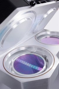
"Eterna" flowable CVD (FCVD) chambers, not showing the many changes from prior PECVD chambers on the Producer platform (source: Business Wire)

Applied Materials' “Eterna” flowable CVD (FCVD) dual-chambers, not showing the many sub-system changes from prior PECVD Producer chambers. (source: Business Wire)

Yesterday, Applied Materials released a flowable CVD (FCVD) process running in new PECVD “Eterna” chambers on the Producer dielectric deposition platform (figure). Targeting 32nm node and beyond ICs with >30:1 AR structures, the FCVD process completely fills gaps from the bottom up with a dense carbon-free silica glass. The FCVD oxide gap-fill process uses secret process chamber sub-systems and a mysterious carbon-free silicon-precursor.

The company says that the chamber had to be significantly re-designed to handle the unique recipe requirements of the precursor and the “flowability.” Standard PECVD chambers reportedly fail in trying to produce FCVD films. “We had to do some unique hardware designs to allows this precursor to go on to the wafer, fill gaps, and leave no carbon in the final film,” said Bill McClintock, Applied Materials’ vice president and general manager of dielectrics and CMP. Consequently, even though it is only matter of time before word leaks out as to which precursor is used, McClintock is confident that OEM competitors will have difficulty in trying to clone the process.

Like Novellus’ CFD silica film, the Applied Materials FCVD silica compares favorably to thermal oxides in terms of density and electrical properties. Unlike the CFD, FCVD is touted as “the ultimate gap-fill dielectric” due to it’s ability to flow into and fill extremely re-entrant structures as narrow as 5nm without voids (figure). Initially targeting DRAM isolation, the FCVD process has past beta-site evaluations at six different end-user fabs for both memory and logic applications. “Every major memory customer has taken one of these,” said McClintock. “They are qualifying them for their major products, whether they be DRAM or NAND.”
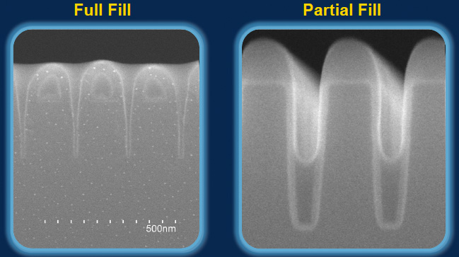
Flowable-CVD (FCVD) provides bottom-up gap-filling with silica using a carbon-free precursor. (source: Applied Materials)

Flowable-CVD (FCVD) provides bottom-up gap-filling with silica using a carbon-free precursor. (source: Applied Materials)

For 32nm node processing, the thermal budget for logic is ~400°C while that for NAND Flash is ~300°C. The basic process flow for any gapfill starts with liner deposition, then FCVD or SOG, then anneal(s), then CMP. The main advantage of FCVD over SOG is that a single FCVD anneal step replaces >10 SOG anneal steps. Applied Materials says that the CoO for 32nm node SOG gapfill is ~$20/wafer, with ~$5/wafer from the precursor cost alone. “We’ve worked with the chemical precursor supplier and the material cost per gram is about one-third of the precursor cost of SOG,” said McClintock. However, due to more efficient use of precursors in CVD compared to SOG tools, the actual cost-per-wafer for the FCVD precursor is hinted to be in the US$1.00-1.50 range.

In response to a question regarding the number of FCVD tools needed to support a high-volume fab, the company claimed that for a 22nm node Flash line running 120K wafer-starts-per-month (WSPM) a “couple of tools” would be needed to deposit a desired layer. If we assume 60K WSPM and 30 working days at 20 hours/day, then the throughput for a 6-chamber Producer would be 100 wafers/hour.

Possible FCVD precursors

Trying to pry “proprietary” information out of a technology executive these days is like trying to pull teeth on a roller-coaster: nearly impossible and always awkward. No OEM wants to talk about any real details today. Applied Materials will not say anything about the precursor molecule, oxidizer or possible catalyst used, continuous or pulsed flows, intermediate molecules formed for flowability, or annealing conditions. In private conversation with BetaSights during the official product launch in Santa Clara yesterday, McClintock provides only the single hint that, “The precursor never sees the plasma.”

Company executives have been careful to say that the precursor enters the chamber as a vapor, and initially deposits on the surface in a “liquid-like” manner to provide the great gap-fill. Then plasma is somehow used to transform the flowable material into a solid silica, perhaps in the presence of an oxidizer and/or a catalyst. The Eterna deposition chamber reportedly requires many unique sub-systems and will cost more than other Producer chambers. However, the company claims at least 50% improvement over SOG in terms of CoO for 32nm node and below gapfill.

We may speculate as to possible carbon-free silicon precursors by reviewing the latest catalog of off-the-shelf specialty molecules from established specialty materials suppliers. SAFC Hitech sells both trichlorosilane (“TCS”, SiCl3H) and silicon tetrachloride (“STC”, SiCl4). Air Liquid lists both hexachlorodisilane (“HCDS”, Cl3Si-SiCl3) and trisilylamine (“TSA”, Si3H9N). Online search reveals that Samsung filed for IP on HCDS for low-temperature conformal oxide deposition in 2002, specifying the use of a Lewis Base (such as pyridine or trimethylaluminum) as catalyst and H2O vapor as reactant in a quasi-ALD sequence.

The only thing we know for sure is that Applied Materials claims sole ownership of the FCVD process, and that the process recipe comes free with the purchase of hardware as is standard with industry CapEx terms and conditions. The precursor is commercially available from a single-source today.

Previous FlowFill dielectric

During the Eterna launch event, ever-alert analyst Dean Freeman of Gartner/Dataquest asked about the comparisons between FCVD and the decade-old “FlowFill” dielectric that had been developed by Trikon. What is now part of the STS division of Sumitomo Precision Products (formerly Aviza, formerly Trikon) had failed to launch a flowable CVD dielectric oxide called “FlowFill” that was based on methyl groups. The product claim by Trikon for FlowFill—a “bottoms-up” dielectric fill for device isolation—was nearly identical to the current product claims for Eterna FCVD. The huge difference is that the latter film uses a carbon-free precursor and a more complex recipe to ensure that there is as little carbon as possible left in the final post-annealed material.

Why did FlowFill fail to win over major customers? Siemens reported in 1998 that the material demonstrated reduced reliability compared to SOG. LSI Logic worked with FlowFill, but then became a fabless company and the non-standard unit-process was not picked up but foundries. Perhaps the residual carbon contamination really was excessive, and there was no easy way to anneal it out. Perhaps it was just ahead of it’s time, since FCVD is now touted for 32nm node and below processing there was probably little pull from fabs to replace legacy CVD processes until now.

The future of IC fabrication seems to be more and more based on integrated thin-film depositions and etches (less and less based on simple 2D shrinks). Specialized new tools and materials are being developed to meet the precise needs of high-volume manufacturing. While the capabilities of legacy tools and processes continue to improve, inflection points routinely arise when something completely new suddenly wins the cost:performance tradeoff. With the introduction of CFD and FCVD for oxides, fab process engineers have new tools to use in creating ever more powerful and compact ICs. It is likely that the same tools can be extended to create SiON and SiN films, too. E.K.

Tuesday, August 17th, 2010

While “Sturtevant’s Law” (which states that optical lithography can make all the circuit structures needed for the next 7-10 years) still may apply, the real limits to any manufacturing technology are financial, not technical. The multiple patterning techniques contemplated for fabricating the next nodes are approaching financial unfeasibility (see BetaBlog post “Steady as she goes: Optical Lithography). Ten years will take us to the 11nm node or beyond. To deal with this impending disconnect, the industry has been investing in various post-optical lithography schemes including extreme ultra-violet (EUV) illumination, e-beam direct write (EbDW), and nano-imprint lithography (NIL). Progress was reported for all these methods at SEMICON/West 2010, but none seemed about to triumph.

ASML getting ready for HVM with EUV

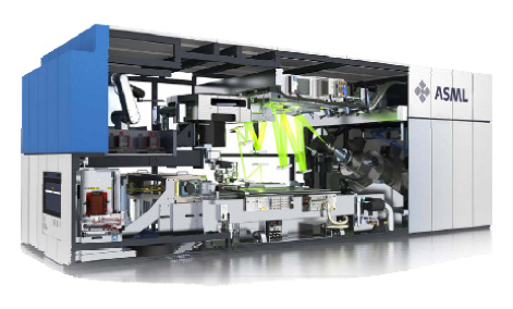
The leading candidate for next-node patterning continues to be EUV lithography (EUVL) using 13.5nm radiation. Hans Meiling of ASML reviewed the company’s extensive progress towards high volume manufacturing with the NXE:3100 EUVL system and follow-on designs. There are three of these NA=0.25 tools already built at ASML and 3 more being assembled. The first laser produced plasma light source has been attached to a 3100 exposure tool and “first light” (slit exposure) achieved.

ASML 2nd Generation NXE:3300B EUVL tool scheduled for first shipment early in 2012 (source: ASML)

ASML 2nd Generation NXE:3300B EUVL tool scheduled for first shipment early in 2012 (source: ASML)

Exposure power is 20W now, but a path has been defined for a 5X upgrade. The collector performance was reported as stable. While an NA=0.25 will likely have resolution sufficient to print ~27nm chips, getting to 22nm and beyond will require higher NA and some resolution enhancement trickery.

Thus ASML has begun work on the NXE:3300 series (figure), which will feature a 0.32 NA projection system and off-axis illumination capability. The NXE:3300B is scheduled for release early in 2012 and is targeted for 125wph throughput. However, achieving that will require a source 12X more powerful than has been demonstrated, Meiling concedes.

Direct Write Alternative

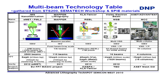
E-beam Direct Write (EbDW) lithography would appear to be a solution to the resolution limit of immersion steppers and the throughput limits of EUV, but the throughput of foreseen EbDW installations is still seen as hideously low. Laurent Pain of CEA-Leti reviewed the progress made by two European efforts: PL2 at IMS in Austria, and Mapper in the Netherlands. Three other programs exist elsewhere (figure).

Developing multi-beam EbDR tools (source: DNP)

Developing multi-beam EbDR tools (source: DNP)

PL2 operates at 50kV and 200X demagnification and has demonstrated 25nm half pitch. The aperture plate in today’s prototype produces 2500 individual beams, of which 90% work properly, according to Pain. Still, getting 6 wph throughput would require an installation with 76 e-beam columns (one for each exposure field) and 256,000 beams per column.

Mapper would require only 13,000 beams at 5kV, but the present prototypes operate only 110 beams…with a throughput of 0.002wph. Going to 10wph requires getting all the beams to work and raising the beam current 40X. If that could be achieved, a cluster of 10 Mappers would use less floor-space than an EUV tool and yield 100 wph. Most likely, though, EbDW would be used first for the line-cut lithography in a spacer multiple patterning scheme since the duty factor would be low, speeding throughput for the <22m cuts.

Mask making gets some attention

The mask making industry stands to benefit from developments in EbDR, according to Naoya Hayashi of DNP, since a workable wafer writing tool can be modified to write 4X masks with little difficulty. However, mask writing is no longer the cost driver or throughput gate for mask-making. Rather, inspection has taken over as the time-sink and largest expense.

Hayashi predicted that optical lithography (with very complex patterns) will likely continue to dominate for logic chip production, but other technologies like EUVL and imprint will pose different and unique challenges for mask makers if they are adopted by some industry segment. Developing the proper tool sets and processes in time will be a challenge for mask makers if there is no industry consensus. Hayashi suggested that device manufacturers and tool vendors should include mask makers in collaborations to find workable next-generation patterning solutions.

Imprint pressing on

The only pattern transfer technology that will avoid design restrictions at 11nm is imprint, according to Ben Eynon of Molecular Imprints Inc., who also predicted that NIL’s cost of ownership will be independent of resolution! MII is overcoming the limitations of its J-FIL technology and Eynon expects to see memory production with it ramp in 2012 or 2013. Defectivity is now <1/cm2 in a clean-room environment, according to Eynon, and mix-and-match overlay <12nm has been achieved using template squeezing with force sensor feedback.

NIL infrastructure issues were being addressed: E-beam inspection and repair tools for the 1X master templates exist as does a capable cleaning tool. Master masks can be written slowly today at 14nm resolution with a 100kVGaussian E-beam tool, but a faster vector-scan will do 22nm. The master masks are being replicated with <20nm half pitch in MII’s TR1100 template production system. With replication, the cost of production with imprint is ¼ that of immersion double patterning and ½ the projected cost of EUV, according to Eynon. The first MII 5XX series pre-production lithography system was shipped in July.

In 2005, Ken Rygler (then the chief marketing officer of MII) bet Brian Grenon that 193nm exposure would be used for 22nm node production, with Grenon betting that something else would be needed, possibly imprint. The time is coming to find out who was right. That the issue is not already decided is a testament to the cleverness of the optical lithography community and the difficulty of every post optical alternative.—M.D.L.

Thursday, August 5th, 2010

Steady but undramatic progress was the theme of lithography presentations at SEMICON/West this year, not that anything more had been expected. In fact, most of the main lithography companies had decided to give the show a miss this year. TEL was the one company that had a full-scale booth, and there was a process to sell: pitch quartering! According to Masayuki Tomoyasu, chief engineer of overseas process development, TEL has a suite of equipment to fabricate 11nm half-pitch (HP) patterns in a cost effective way. Doing 22nm, the next step in Moore’s Law, would only take half the effort. Improved double-patterning results were also revealed by IMEC/ASML and by Nikon.

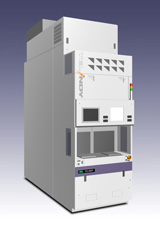
TEL Telindy Plus ALD tool (source: TEL)

TEL Telindy Plus ALD tool (source: TEL)

TEL’s resist core transfer process is a variation on self-aligned sidewall double patterning, where a “core” is fabricated by standard 193nm immersion lithography, trimmed and etched, then gets coated with a sidewall material (which becomes the circuit pattern) and is finally removed. However, the TEL sidewall material is ALD SiO2, deposited at low temperature on the resist itself, before any etching into a transfer layer.

So, after a wafer with a 40nm half-pitch resist pattern comes out of a coat-develop track, the resist and BARC (and maybe a sacrificial layer) are trimmed to 20nm CD in a TEL Tactras Vigus etcher and then conformally coated with SiO2 at low temperature in a TEL Telindy Plus ALD system (figure). The Tactras Vigus then performs an etch-back on the SiO2 film to open the core, etches and strips out the resist/BARC, and transfers the sidewall pattern into the hard-mask. A post-etch clean in an asher completes the process, leaving a 20nm HP grating. According to Tomoyasu, TEL showed SEMs of its own internal 300mm wafer results, not those of a customer.

To get to 11nm, the process begins at 44nm HP, and uses the ALD SiO2 flow described above—on either the photoresist or an underlying core material—to get to 22nm HP structures. Then another ALD of SiO2 forms new sidewalls. Finally, another multistep plasma etch process opens the tops of the conformal sidewall, removes the cores and etches the second sidewall pattern into the hard-mask. A final clean leaves an 11nm HP line-space pattern on the wafer. Edge-on SEMs showed >3:1 aspect ratios with near 90 degree profiles and good regularity. Any such multi-step process needs to be validated with extensive CD metrology and statistics, but these results indicate that 11nm is no longer a fantasy…if one can pay for 3 etches and two depositions!

Designing for double-patterning

Of course, any layout has to be drawn before it is quartered. Designing layouts that can be fabricated by such “lost-core” techniques is a challenge, but no more so than any other feasible litho method below ~65nm CD. At the Advanced Lithography Symposium held July 14 at the North Hall TechXPOT, Jongwook Kye of Global Foundries described the Design-Technology Co-Optimization (DTCO) necessary for today’s circuit scaling.

According to Kye, his “transdisciplinary” optimization is not a new idea: designers have been trying to accommodate process realities since 90nm when poly went unidirectional. Interdisciplinary communication has just produced more restrictions. At 65nm the active layer became unidirectional, and at 45nm the contact landing pads went away and poly CD became uniform. Double patterning first appeared at 32nm and now we are looking at 22nm. Interdisciplinary collaboration has become essential because the litho process choice and the decomposition for double patterning will become chip- and layer- dependent, with no single optimum method.

Don’t forget old fashioned immersion

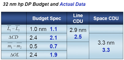
DP budget and actual results achieved with a Nikon NSR 620D immersion stepper. (source: Nikon Precision)

At the Sokudo Litho Breakfast (ably blogged about by Toppan Photomask’s chief technology officer Franklin Kalk), Steve Renwick of Nikon predicted that process development for EUV high volume manufacturing would be delayed until 2015 due to infrastructure issues, and thus the semiconductor industry will need a bridge technology. That technology would have to leverage today’s 193nm immersion exposure tools with double patterning flows.

Source mask-optimization (SMO) with single exposure can give better process windows, but not sub-80nm pitch resolution. So, to get to 32nm HP and beyond, one needs control of CD and image placement. Renwick claimed that the Nikon NSR-620D has met the requirements for 32nm HP (figure) and also demonstrated 20nm HP lines and spaces.

IMEC, the Belgian R&D consortium, separately announced the double patterning results obtained with an ASML XT:1900i immersion stepper equipped with a FlexRay freeform illuminator (figure). Optimized freeform illumination approaches the limits of immersion lithography in geometries where traditional illumination modes cannot. The FlexRay uses a programmable array of thousands of individually adjustable micro-mirrors to create any pupil shape in a matter of minutes (see BetaSights’ exclusive prior coverage of ASML’s “Holistic Lithography”).

Comparison of ASML illumination sources for double patterning of a contact layer along with the images produced, and a table comparing exposure latitude (EL), depth of focus (DOF) and mask error enhancement factor (MEEF). The final hard-mask pattern is at right. (source: IMEC)

Comparison of ASML illumination sources for double patterning of a contact layer along with the images produced, and a table comparing exposure latitude (EL), depth of focus (DOF) and mask error enhancement factor (MEEF). The final hard-mask pattern is at right. (source: IMEC)

The demonstration announced was the contact and metal layer for a 22nm node SRAM of 0.078µm² bit cell area done by LELE double patterning into a hard mask, with the application of simultaneous source – mask optimization (SMO) and FlexRay illumination. The asymmetric X Y positions of the freeform poles cannot be mimicked in a standard source, but would require a custom diffractive optical element likely requiring weeks to deliver.

Stay tuned for a future blog posting about recent EUV, EbDW, and NIL developments.—M.D.L.

Wednesday, July 21st, 2010

After at least a year of being in denial, Applied Materials (AMAT) finally acknowledged some of the reality that there is no market for 6% efficient photovoltaic (PV) fab lines, and killed the “SunFab” that has been sold to unfortunates over the last few years. With no new customers expected, and old customers going bankrupt or having to retool lines to stay running, these thin-film amorphous-silicon (TF a-Si) on glass turnkey production lines are clearly not capable of keeping up with 20% efficient crystalline-silicon (c-Si) and 10% efficient TF technologies. However, the company CEO refuses to acknowledge any mistakes, says they’ll fill the backlog, and claims that, “competitive pressures from crystalline silicon…did not allow the market to take off.” First Solar shipped ~1GW of ~10% efficient TF PV in 2009. The market took off, just not with SunFabs.

AMAT chairman of the board of directors, president, and CEO Mike Splinter further asserted that, “SunFab is a remarkable product. Unlike anything we have done before, it is an example of the kind of revolutionary innovation that Applied Materials is capable of producing. In just a few years we developed a turnkey solution, successfully executed our technology roadmap, achieving greater than 10% stabilized module efficiency and silicon uniformity across the 5.7 square-meter substrate.”

The above quote—part of Splinter’s online video non-acceptance of responsibility—is an amazing example of corporate double-speak, in that each sentence is factually correct while evading key facts. In recent months the world has seen the CEOs of BP, Toyota, and Apple issue various official statements to deal with problems; evasive corporate positioning statements never help in the end.

Let’s examine Splinter’s evasions in some detail:

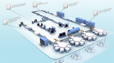
  1. Quickly developed a turnkey solution – by cobbling together old in-house FPD tools with pricey technology acquisitions the company did offer a turnkey line (figure)…where just the tool depreciation costs alone could be estimated to add $0.60/W to manufacturing cost (see below).

  2. Successfully executed the technology roadmap – while utterly failing to execute on a business roadmap that could provide competitive products to the market.

  3. Achieved >10% stabilized module efficiency – sure, downhill with the wind on a good day in the lab at extra cost for dual- and tri-layer materials stacks…while routine cost-effective fab results remained at 6% for a single layer.

AMAT will, of course, continue to try to sell over-priced support services to the unfortunates who bought SunFabs, so some of the people who had been working in the PV division will be moved over to the “Repairs & Spares” division. The company’s Xi’an, China PV R&D center will cease working on TF technology and will focus on mc-Si and c-Si wafers instead. The c-Si PV tools sold by AMAT—essentially all of which were acquired over the last four years—continue to do well in the market. Still, the company will likely lose hundreds of employees and will write-off ~$400M. Mark Pinto will remain in charge of PV products as executive vice president and general manager of the Energy and Environmental Solution (ESS) group, while also remaining as CTO of AMAT Corp.

In the video Splinter said, “Innovation is the heart of our company. We’ll take the lessons from SunFab and use them to make us stronger.”

What lessons might we learn from SunFab?

  1. If you supply technology, don’t bet the company against innovation. When AMAT launched SunFab it was a bet that innovation in thin-film PV would not succeed. Choosing 6% efficient and mature a-Si technology in 2006 was a bet against less-mature CdTe and CIGS thin-film technologies (had First Solar failed to develop $1/Wp with 10% efficient CdTe then things might be different for a-Si in 2010).

  2. If you buy technology, don’t bet the company against innovation. After betting the company on a SunFab line, Sunfilm AG in Grossroehrsdorf, Germany filed for bankruptcy protection on March 26 of this year. After buying a standard (40MW/year @ 6% efficiency) SunFab, Moser Baer in Greater Noida, India (also with 80MW/year c-Si cell/module fab capacity) had to idle the TF line for much of 2009 while working to customize it such that it could deliver ~7% efficiency. Signet Solar in Dresden, German used over a year of depreciation of a SunFab line to deliver a grand total of 10MW to the field, while it also did it’s own upgrade to ~7% efficiency.

  3. Do the math. A basic 40MW/year capacity SunFab line was priced at ~US$120M; assuming 5-year linear depreciation, this results in $0.60/W just to pay for the cost of equipment depreciation! Considering the rule-of-thumb that the module cost is ~60% of the total installation cost, and that total cost scales with the area to be installed, and that First Solar’s ~10% efficient modules set $1/W price-points for TF, it seems that you would have to sell 6% efficient a-Si panels for $0.60/W to try to complete…the same price you pay just to own the tooling! Maybe a vertically integrated company building solar farms like T-Solar can afford to run a SunFab line at a loss, but even they might see reduced farm costs with buying mc-Si or c-Si modules on the open market.

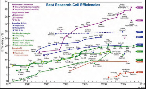
(Source: NREL, 2007)

(Source: NREL, 2007)

Research efficiencies (figure) are not the same as fab efficiencies, but the more mature the technology the closer fab efficiencies are to their practical limits. When SunFab was conceived, the maximum lab result was 12% for a-Si TF PV, and having already been run in fabs for decades was known to result in ~6% efficiency in production. In contrast, while both CdTe and CIGS had been explored in labs for decades with champion results reaching to 16-18%, fab processes were still relatively immature and could thus be expected to improve significantly over time from ~6%.

The reality of the PV module market is that CdTe and CIGS TF technology suppliers continue to innovate in their fabs, with First Solar leading the way down the $/W learning curve. Fabs still trying to run a-Si at 6-7% efficiency face a serious gap compared to ~10%, and stacking a multi-crystalline (mc-Si) TF over the a-Si to create a more expensive “tandem junction” really only provides 8-9%.

In the analysts’ question-and-answer sessions today, AMAT executives continue to assert that tandem junction TF will win in the market when a-Si fails, so that the company will sell new mc-Si CVD tools to old a-Si SunFab lines eventually. However, if the cost/benefit argument is valid for a-Si/mc-Si TF then why wouldn’t all customers opt for this today?

The only reason AMAT has a story to tell in PV today is because of the acquired portfolio of c-Si OEMs. With SunFab, Splinter effectively bet the company against thin-film innovation. How sad and ironic for a company that was built on thin-film technology innovation (for IC fabs).

There are thousands of hardworking engineers and technicians who’ve lost years of their lives by mistakenly working on SunFab, both within AMAT and at customer sites. Investors into companies buying SunFab lines stand to lose hundred of millions of dollars. The entire PV industry loses credibility when AMAT’s SunFab is added into high profile technology blunders like Nanosolar. What have we learned again? -E.K.